
The emerging force in the semiconductor field: entering the world of glass wafers
In the current rapidly developing semiconductor and optical industries, in addition to the well-known silicon wafers, glass wafers are emerging as an important complementary material to silicon wafers due to their unique performance advantages, and are widely used in various cutting-edge fields such as microelectronics, optical devices, and smart wearables. This circular thin sheet made from ordinary glass, quartz, alkali free glass and other raw materials may seem simple, but it is the key cornerstone that supports the operation of many high-end technological products.
Glass wafers are a new type of precision product that emerged in response to the development of semiconductor and optical technology, with quartz glass wafers being the most widely used category. Compared with traditional quartz glass lenses, the production standards for glass wafers are very strict. Not only is the thickness thinner and the size specifications richer, but the processing accuracy and surface smoothness have also reached the level of high-end semiconductor applications. It has many excellent characteristics: strong resistance to chemical corrosion, able to resist the erosion of various chemical reagents; Excellent thermal stability, able to adapt to complex working conditions with alternating high and low temperatures; The extremely low surface roughness and ultra-high light transmittance enable it to smoothly penetrate multiple application fields such as semiconductors, optics, and consumer electronics.

According to the differences in production process and optical performance, mainstream quartz glass wafers can be divided into three categories, each suitable for different usage scenarios. The synthesis of hydroxyl containing far ultraviolet quartz glass is made by chemical vapor deposition method, with high hydroxyl content, low metal impurities, and outstanding radiation resistance. It is mainly used in the field of far ultraviolet optics. Gas refining optical quartz glass is formed by hydrogen oxygen flame technology, with high chemical purity and excellent ultraviolet transmission performance, making it the mainstream choice in the electronics and semiconductor industries. Vacuum melting infrared optical glass is made by melting in a vacuum high-temperature environment, with extremely low hydroxyl content and low absorption of infrared light. It is suitable for infrared related scenes, but its ability to transmit far ultraviolet light is relatively weak.
In terms of physical performance, quartz glass wafers also exhibit outstanding performance. Its melting point can reach 1713 ℃, and its softening point is about 1580 ℃. Its high temperature resistance can fully cope with various high-temperature processes in semiconductor production. Its thermal expansion coefficient is extremely small, and it is not easily deformed in high temperature environments. At the same time, its electrical performance is stable, and even at high temperatures, it can still maintain high dielectric strength and low signal loss, making it very suitable for making high-frequency circuits and insulating substrate materials. In addition, the viscosity of glass wafers is affected by the content of hydroxyl groups and impurities, which has become an important basis for controlling product quality in the production process.
Nowadays, the application scenarios of glass wafers have become increasingly diverse. In the field of semiconductors and microelectronics, it is the core processing substrate for microelectromechanical components, image sensors, microwave circuits, and IoT arrays. In wafer level packaging and fan out wafer level packaging processes, it is often used as a carrier for silicon wafers and has outstanding advantages in wafer thinning. In the traditional optical field, glass wafers can be processed into basic optical components such as prisms and lenses. In the field of consumer electronics, it is also a key component of augmented reality and mixed reality smart wearable glasses. In addition, it can also be used as a substrate for various display screens, and is also applied in products such as wafer level lenses, car lighting components, biometric modules, etc., deeply integrated into daily life.
From the perspective of the complete industry chain, the division of labor in the glass wafer industry is clear and distinct. The upstream mainly focuses on the mining and purification of basic raw materials such as quartz sand; The midstream is the core production process, where raw materials are processed into finished wafers of different sizes and specifications through multiple processes such as melting, cutting, grinding, and precision polishing; Downstream, it connects with terminal markets such as displays, semiconductors, and optical devices, forming a complete and mature industrial system.
With the continuous iteration and upgrading of microsystem technology, high-end semiconductor packaging, and intelligent optical equipment, the demand for glass wafers in the market is still rising. As a high-quality partner of silicon wafers, glass wafers, with their irreplaceable optical, thermal, and electrical properties, will undoubtedly unleash their potential in more high-tech fields and become an important new material to promote the sustainable development of related industries.
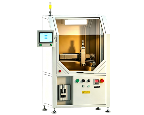
Ultrasonic wafer coating equipment serves as an alternative to traditional spin coating for semiconductor manufacturing, delivering superior thin-film consistency, accurate process regulation and far higher raw material utilization in photolithography workflows. Standard spin coating struggles with uneven coverage on wafers featuring steps, grooves and recessed cavities, resulting in inconsistent layering of photoresist and dielectric substances. Precision ultrasonic spraying overcomes this flaw, forming flawless, evenly distributed films on intricate wafer surface structures and multiple base materials such as silicon and ceramic wafers.
Engineered to fit standard cleanroom environments, non-contact ultrasonic spray equipment generates stable low-speed atomized coatings with adjustable thickness and strong interfacial adhesion. The technology fits numerous semiconductor production scenarios: MEMS coating, photoresist deposition, polyimide dielectric film formation and protective layer coating prior to wafer cutting, and can be scaled flexibly from laboratory research to fully automated high-volume manufacturing lines.
Substituting spin coating with ultrasonic spraying improves coating homogeneity and layer durability while cutting chemical usage significantly. This process addresses core industry demands, including elevated production yields, finer microscale feature fabrication and eco-friendly semiconductor manufacturing operations.
About Cheersonic
Cheersonic is the leading developer and manufacturer of ultrasonic coating systems for applying precise, thin film coatings to protect, strengthen or smooth surfaces on parts and components for the microelectronics/electronics, alternative energy, medical and industrial markets, including specialized glass applications in construction and automotive.
Our coating solutions are environmentally-friendly, efficient and highly reliable, and enable dramatic reductions in overspray, savings in raw material, water and energy usage and provide improved process repeatability, transfer efficiency, high uniformity and reduced emissions.
If you have any technical questions, customization demands, or procurement inquiries about ultrasonic atomization nozzles, feel free to contact our professional sales and technical team for detailed parameters, customized solutions, and industry application support.
Email: market2@cheersonic.com
