
A Comprehensive Analysis of Semiconductor Wafer Technology
Semiconductor wafer technology forms the physical foundation of modern digital civilization. From smartphones to AI computing clusters, every chip begins as a seemingly ordinary silicon wafer.
The wafer’s journey begins with high-purity monocrystalline silicon. Silicon ingots grown via the Czochralski process are sliced into thin wafers by precision wire saws; subsequent grinding, etching, and polishing yield mirror-like wafers with surface roughness controlled at the nanometer scale. This “blank canvas” serves as the substrate for hundreds of subsequent manufacturing steps.
At the heart of wafer manufacturing lies a precise, cyclical process. Photolithography is the “soul” of the operation: ultraviolet light projects circuit patterns through a mask onto photoresist, defining nanometer-scale features. Next, plasma etching removes excess material, “sculpting” the pattern into form. Doping—often via ion implantation—alters local conductivity, endowing transistors with switching capabilities.
As manufacturing processes advance to the 3-nanometer node and beyond, challenges intensify. In extreme ultraviolet (EUV) lithography, stochastic photon effects can cause random pattern failures, severely impacting yield. To counter this, the industry has adopted techniques such as self-aligned double patterning, utilizing sidewall spacers to achieve finer pitch division. Meanwhile, chemical mechanical polishing (CMP) planarizes the wafer surface to an atomic level after each layer is completed, ensuring precise alignment for multi-layer stacking.
Defect detection and yield control are integral throughout the process. Machine learning-based defect detection systems identify minute anomalies that traditional optical inspection misses, pinpointing the root causes of yield loss within vast datasets. Precision coating technologies, such as ultrasonic spraying, offer new solutions for applying photoresist uniformly over complex 3D structures.
Looking ahead, the integration of 2D materials at the wafer scale is being explored, promising to open new pathways for the post-Moore’s Law era. Simultaneously, the industry continues to expand; the demand for AI computing power keeps advanced process lines running at full capacity, while mature process sectors are undergoing a restructuring of supply and demand dynamics.
The journey of a single wafer represents a profound convergence of materials science, precision engineering, optics, and artificial intelligence. It carries not merely transistors, but the fundamental logic underpinning the entire intelligent era.
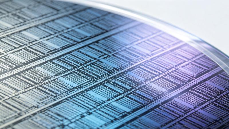
Semiconductor Wafers Technology
Semiconductor Wafers Technology An accessible yet in-depth look at [...]

The emerging force in the semiconductor field: entering the world of glass wafers
The emerging force in the semiconductor field: entering the world [...]
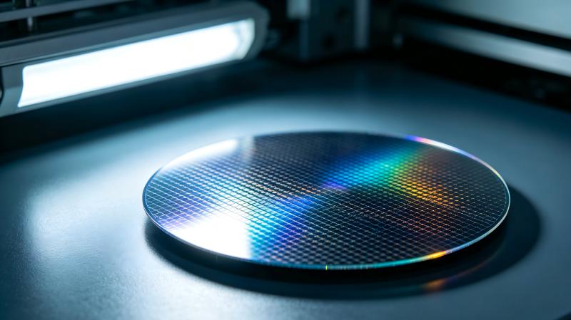
Precision Insulation Dielectric Coating Solution
Precision Insulation Dielectric Coating Solution Semiconductor wafer polyimide ultrasonic spraying [...]
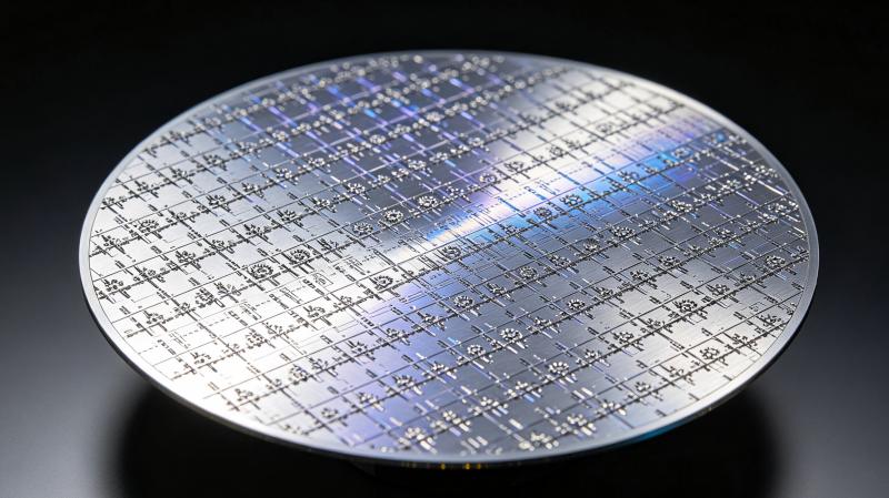
Semiconductor Wafers Coating Knowledge
Semiconductor Wafers Coating Knowledge Comprehensive guide to semiconductor [...]
To reach our anytime via email please fill out the form below with your request and a company representative will reply to you. To find your local CHEERSONIC representative to connect directly click your region in the contact drop down menu.

Contact CHEERSONIC For immediate assistance please contact us the corporate headquarters during business hours at 6:00 am – 22:00 pm.
Tel: 0571-87910406
- Mobile: +86 15869049660
- Email: Market2@cheersonic.com
Add: 11-13 Chuangye Road, Changkou, Fuyang, Hangzhou, Zhejiang, China
