
Semiconductor Wafer Coating
Wafer-Level Ultrasonic Coating for Semiconductors
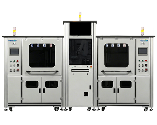
Ultrasonic wafer coating equipment serves as an alternative to traditional spin coating for semiconductor manufacturing, delivering superior thin-film consistency, accurate process regulation and far higher raw material utilization in photolithography workflows. Standard spin coating struggles with uneven coverage on wafers featuring steps, grooves and recessed cavities, resulting in inconsistent layering of photoresist and dielectric substances. Precision ultrasonic spraying overcomes this flaw, forming flawless, evenly distributed films on intricate wafer surface structures and multiple base materials such as silicon and ceramic wafers.
Engineered to fit standard cleanroom environments, non-contact ultrasonic spray equipment generates stable low-speed atomized coatings with adjustable thickness and strong interfacial adhesion. The technology fits numerous semiconductor production scenarios: MEMS coating, photoresist deposition, polyimide dielectric film formation and protective layer coating prior to wafer cutting, and can be scaled flexibly from laboratory research to fully automated high-volume manufacturing lines.
Substituting spin coating with ultrasonic spraying improves coating homogeneity and layer durability while cutting chemical usage significantly. This process addresses core industry demands, including elevated production yields, finer microscale feature fabrication and eco-friendly semiconductor manufacturing operations.
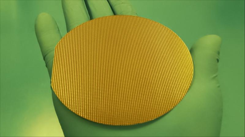
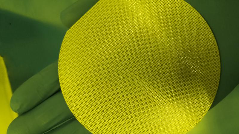
Photoresist Coating Systems for Photolithography Wet Process
Ultrasonic spray methods deliver precisely controlled, even photoresist layers for MEMS manufacturing and photolithography, overcoming common drawbacks of spin coating such as liquid accumulation, surface streaking, and inadequate coverage on steps and sidewalls. It coats patterned wafers featuring deep cavities and high-aspect structures uniformly, offering consistent film quality unachievable with spin coating.
The technology achieves excellent thickness uniformity over complex topographies and reliable photoresist behavior, perfectly fitting MEMS and general wafer-scale photolithography manufacturing needs.

Polyimide Coating
Ultrasonic coating technology produces pinhole-free polyimide insulation layers with flexible thickness control spanning submicron to multiple micron scales, featuring superior step coverage and uniform coating distribution on full wafers. The low-speed spraying mode boosts coating adhesion, cuts material waste and ensures stable, repeatable processing—key advantages for semiconductor wafer dielectric insulation production.
Compatible with common solvents, this coating solution fits seamlessly into cleanroom surface pretreatment and curing production lines. It delivers robust, consistent insulating properties ideal for wafer-level packaging and multi-layer interlayer isolation.

Protective Films for Dicing
Temporary defect-free protective layers can be deposited via ultrasonic spraying ahead of wafer singulation to guard wafers during dicing procedures. The mild contact-free spray method creates uniform, well-adhered coatings that eliminate chipping, cracks and particle buildup. Films can be peeled off cleanly afterwards to maintain elevated manufacturing yields.
Applicable to silicon, ceramic and compound wafer substrates, this protective coating enhances substrate robustness and minimizes surface defects, delivering consistent premium surface quality for semiconductor packaging production lines.
State-of-the-art wafer-scale ultrasonic coating techniques support semiconductor factories in completing precise, even, high-throughput film deposition for photolithography. Adaptable to cleanroom environments, this spraying technology serves diverse use cases ranging from MEMS and dielectric film coating to dicing surface protection. It supplies repeatable, superior coating performance and raises the industry-wide benchmark for semiconductor thin-film processing.
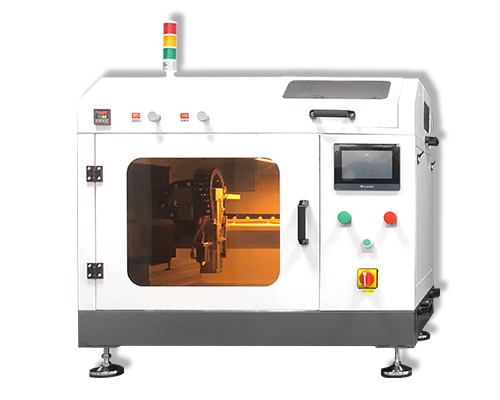
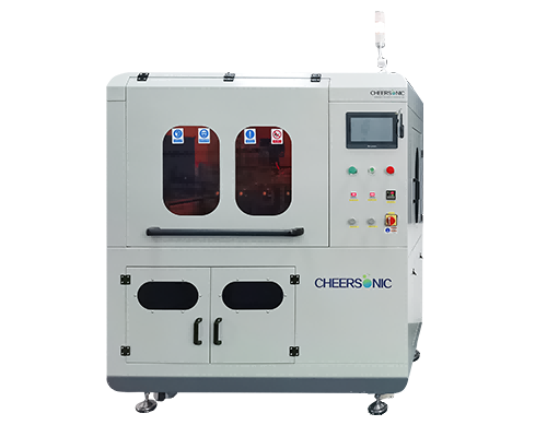
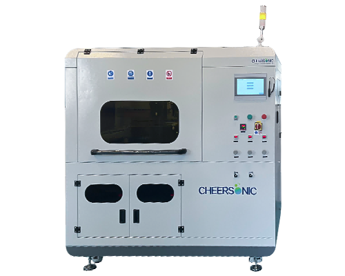
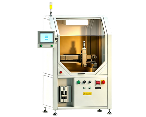
EQUIPMENT SOLUTIONS
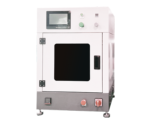
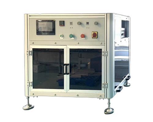
To reach our anytime via email please fill out the form below with your request and a company representative will reply to you. To find your local CHEERSONIC representative to connect directly click your region in the contact drop down menu.

Contact CHEERSONIC For immediate assistance please contact us the corporate headquarters during business hours at 6:00 am – 22:00 pm.
Tel: 0571-87910406
- Mobile: +86 13588732518
- Email: Market2@cheersonic.com
Add: 11-13 Chuangye Road, Changkou, Fuyang, Hangzhou, Zhejiang, China
