
Semiconductor Wafers Coating: Processes, Materials & Key Technologies
Semiconductor wafers are the foundation for manufacturing chips, and coatings are an essential core process in wafer processing. Simply put, a coating is a layer of functional thin film evenly covering the surface of a silicon wafer, commonly including photoresist, dielectric layer, conductive layer, and protective film. The thickness of these films is often only a few micrometers or even nanometers, but it directly determines the performance, yield, and reliability of the chip. Taking photoresist as an example, it is the “photosensitive film” of photolithography process. Whether the coating is uniform and free of defects will directly affect the transfer accuracy of circuit patterns. It can be said that without precise coating technology, there would be no advanced chips today.
At present, the semiconductor industry mainly adopts two technical routes: Spin Coating and Spray Coating. Spin coating is the process of dropping liquid onto a rapidly rotating wafer and spreading it into a film using centrifugal force. It is suitable for flat surfaces, but it results in significant material waste and uneven thickness on wafers with concave convex shapes. Ultrasonic spraying utilizes high-frequency vibration to atomize liquid into micrometer sized droplets, which are then precisely deposited onto the wafer surface at low speed. With high material utilization, it can achieve uniform coating on complex three-dimensional structures, making it particularly suitable for advanced packaging and MEMS devices. In addition, techniques such as chemical vapor deposition (CVD) and atomic layer deposition (ALD) also play an important role in the preparation of specific thin films.
With the advancement of chip processes towards 3nm and 2nm, as well as the rise of advanced packaging such as 2.5D/3D packaging, wafer coatings are facing greater challenges. Large sized wafers (12 inches and above), higher aspect ratio structures, and thinner film requirements are all driving continuous innovation in coating technology. Ultrasonic spraying, due to its non-contact, high-precision, and low waste characteristics, is gradually moving from the research and development stage to the mass production line, showing great potential in fields such as photoresist, flux, and nanomaterials. In the future, coating technology will develop towards greater precision, environmental friendliness, and intelligence, providing solid support for the continuous advancement of the semiconductor industry.
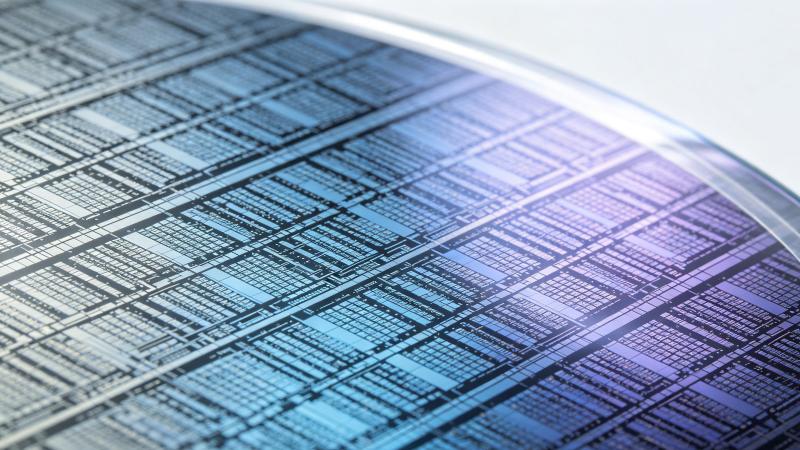
Semiconductor Wafers Technology
Semiconductor Wafers Technology An accessible yet in-depth look at [...]

The emerging force in the semiconductor field: entering the world of glass wafers
The emerging force in the semiconductor field: entering the world [...]
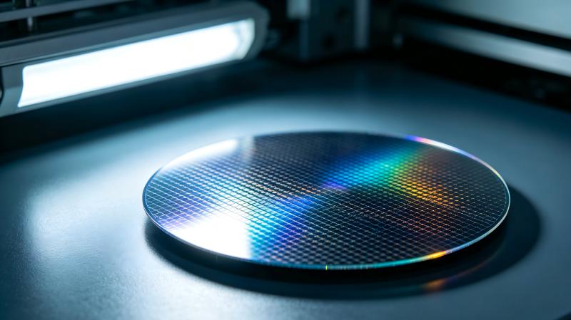
Precision Insulation Dielectric Coating Solution
Precision Insulation Dielectric Coating Solution Semiconductor wafer polyimide ultrasonic spraying [...]
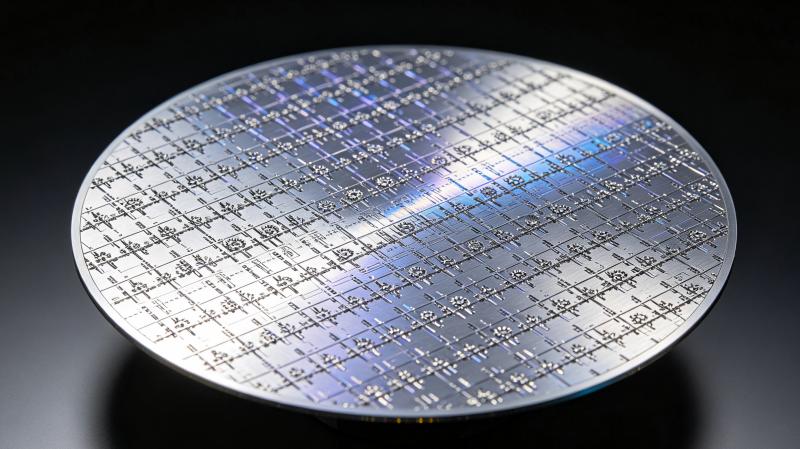
Semiconductor Wafers Coating Knowledge
Semiconductor Wafers Coating Knowledge Comprehensive guide to semiconductor [...]
