
Ultrasonic Spray Photoresist Coating for MEMS Wafers
Ultrasonic spray of photoresist for MEMS wafers and other substrates with varying topographies
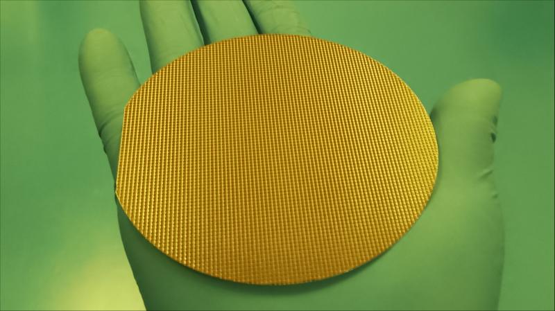
For over ten years, researchers have carried out direct photoresist spraying on MEMS wafers, silicon substrates and assorted three-dimensional microstructures. Extensive studies have validated the merits of this deposition technique when filling deeply etched, tall surface relief structures with photoresist. Compared with traditional spin coating methods, ultrasonic spray photoresist deposition delivers superior coating homogeneity, especially on the upper edge of sidewalls within high-aspect-ratio trenches and V-shaped grooves. When relying on centrifugal force from spin coating, photoresist struggles to evenly cover sidewalls of high-aspect-ratio features; the material tends to accumulate excessively at the base of recessed cavities.
As a straightforward, cost-effective and highly reproducible coating technique for photolithography wet-process photoresist layers, ultrasonic spraying serves as a viable substitute for spin coating when working with wafers that carry intricate surface geometries. This spraying method supports precise regulation over liquid feed rates, coating travel speeds, solvent supply volumes and total photoresist layering output through sophisticated layered deposition logic. Low-speed atomized spray streams can be shaped into accurate, adjustable spray footprints, eliminating redundant material overspray while generating ultra-thin films with consistent coverage across irregular substrate surfaces. Ultrasonic direct spraying has been verified as a stable, high-performance lithography solution for photoresist coating on 3D microstructures, which cuts down component malfunctions caused by metal layers being overexposed to etching chemicals.
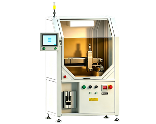
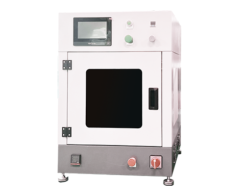
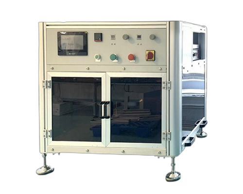
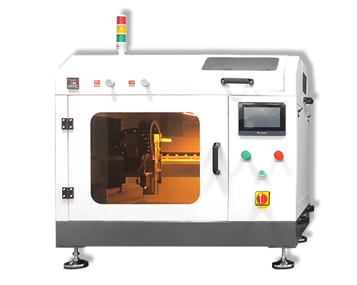
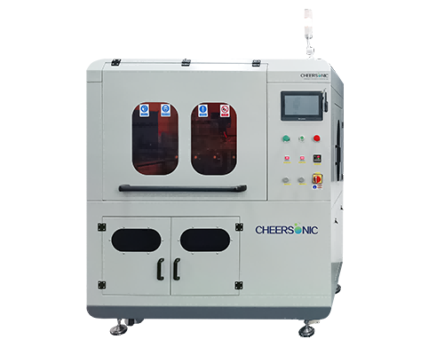
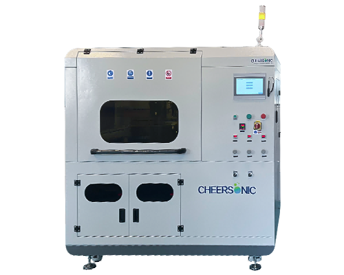
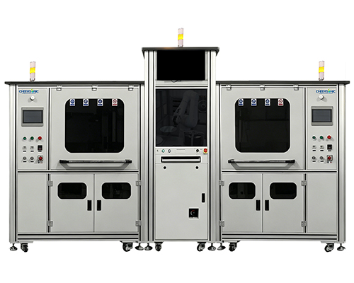
Fully automated wafer processing equipment can accommodate two wafer cassettes holding 100 mm, 150 mm or 200 mm substrates, with compatibility for 300 mm wafers as an add-on configuration. This automated transport unit meets Class 1 cleanroom standards, equipped with pre-positioning workflows, fully unattended wafer loading sequences, and full-featured operational control software. The hardware can be matched with either one standalone coating unit or a dual-unit coating setup as illustrated.
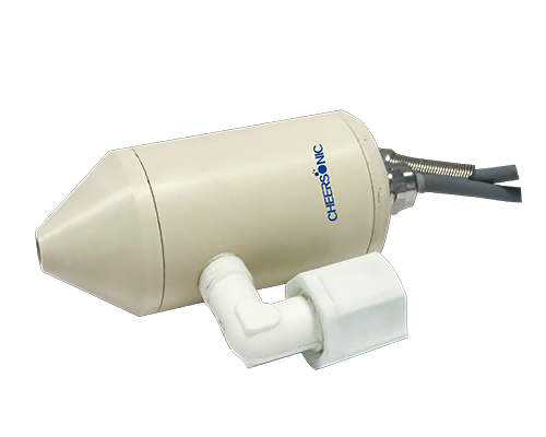
Key advantages of ultrasonic atomizing heads for direct photoresist spraying in photolithography wet workflows are listed as follows:
- Homogeneous ultra-thin photoresist layers across all types of wafer surface contours and uneven substrate geometries
- Consistent, even sidewall coating performance on high-aspect-ratio trench structures
- Clog-resistant atomization that sustains steady photoresist deposition output
- Capacity to form uniform single-micron thin coating layers
- A well-documented coating workflow with outstanding run-to-run reproducibility
EQUIPMENT SOLUTIONS
To reach our anytime via email please fill out the form below with your request and a company representative will reply to you. To find your local CHEERSONIC representative to connect directly click your region in the contact drop down menu.

Contact CHEERSONIC For immediate assistance please contact us the corporate headquarters during business hours at 6:00 am – 22:00 pm.
Tel: 0571-87910406
- Mobile: +86 13588732518
- Email: Market2@cheersonic.com
Add: 11-13 Chuangye Road, Changkou, Fuyang, Hangzhou, Zhejiang, China
