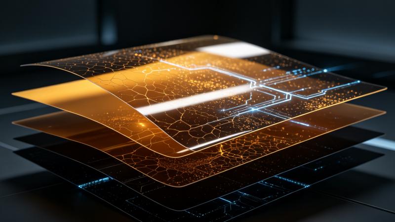
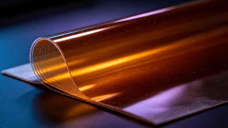
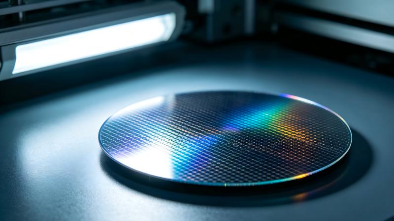
PSPI Photosensitive Polyimide
PSPI Photosensitive Polyimide: A Core Insulating Material for Glass Substrate Packaging, Bridging Panel Technology and Advanced Packaging
As AI computing chips evolve toward higher bandwidth and greater integration, traditional packaging substrates are increasingly revealing limitations such as significant thermal deformation and high-frequency signal loss. Glass substrate packaging—leveraging advantages like low thermal expansion, low dielectric loss, and suitability for large-format panel-level carriers—has emerged as a key technological pathway for next-generation advanced packaging. Within this landscape, photosensitive polyimide (PSPI)—a core insulating material for glass substrate packaging—is successfully bridging the gap between the display panel industry and semiconductor advanced packaging, effectively overcoming material technology barriers between these two sectors.
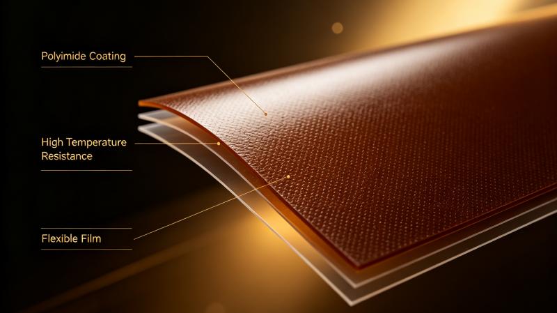
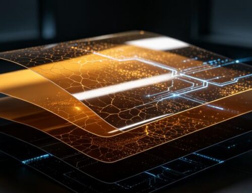
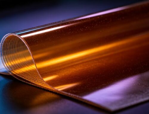
PSPI (photosensitive polyimide) is a functional polymer material created by incorporating photosensitive groups into the polyimide molecular chain. It retains the inherent properties of standard polyimide—such as high-temperature resistance, excellent insulation, chemical resistance, and stress buffering—while adding photolithographic capabilities. This allows for the direct fabrication of fine patterns through exposure and development, eliminating the need for separate photoresists for masking and etching, thereby significantly simplifying manufacturing processes. PSPI has already seen large-scale application in the OLED display industry, serving as a critical dielectric material for planarization and pixel definition layers; the accumulated expertise in coating, photolithography, and defect control provides a solid technical foundation for its expansion into glass-based semiconductor packaging.
Within glass substrate packaging systems, PSPI performs multiple indispensable functions. First, it serves as the interlayer insulation dielectric for Redistribution Layers (RDL); photolithography allows for the precise creation of micro-vias and openings, providing the structural basis for copper wiring and interlayer interconnects, which enables high-density, fine-pitch circuitry. Second, significant differences in the coefficient of thermal expansion (CTE) between glass, metal wiring, and other dielectric layers often lead to interfacial stress during thermal cycling. PSPI’s inherent flexibility acts as a stress buffer, mitigating the risks of interfacial warpage and cracking. Additionally, it can be used for passivation and protection around Through-Glass Vias (TGV), thereby enhancing the overall reliability of the packaged device. The material’s low-dielectric and low-loss characteristics enable it to meet the demands of high-speed, high-frequency signal transmission and satisfy the electrical performance requirements of high-performance computing (HPC) chips.
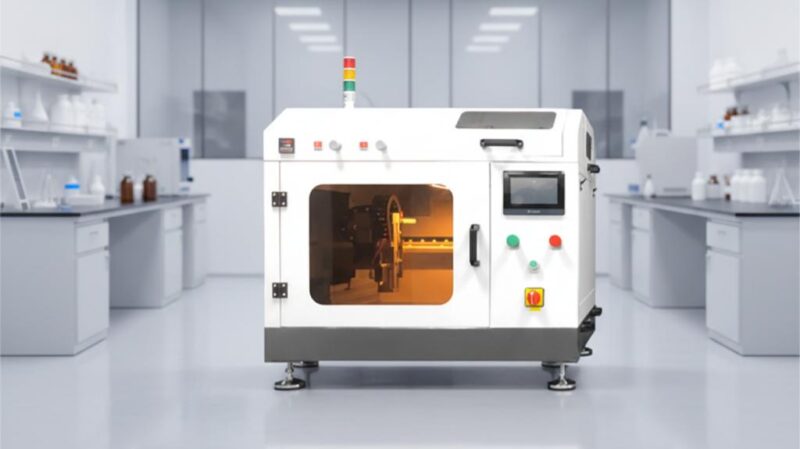
The display industry and glass-substrate packaging processes share significant commonalities; both utilize large-area glass as a base and involve core processes such as coating, photolithography, curing, and thin-film deposition. The PSPI formulations and film-formation expertise accumulated in the display industry can be rapidly transferred to semiconductor packaging applications—a key factor enabling PSPI to successfully cross over into this new sector. Regarding film-formation methods, in addition to spin coating and slit coating, ultrasonic spraying can also be employed to prepare PSPI films; this technique creates a thin, uniform dielectric layer on the glass substrate, meeting the coating requirements for substrates with specific structural features. The complete process typically encompasses substrate pretreatment, application of the PSPI precursor solution, pre-baking, patterning via exposure and development, and finally, high-temperature thermal curing to complete the imidization reaction, resulting in a stable, dense insulating film. Parameters such as curing temperature and the heating ramp profile directly determine the film’s insulation, heat resistance, and adhesion performance.
Naturally, transitioning from display applications to advanced packaging requires performance upgrades for PSPI. Semiconductor packaging imposes far stricter standards than display panels regarding dimensional stability, high-temperature tolerance, ionic impurity levels, and film retention rates. Consequently, molecular modification and formulation optimization are essential to reduce internal stress and impurity ions, ensuring the material can withstand semiconductor processing steps such as multiple high-temperature reflow cycles and plasma treatments. As glass-substrate packaging targets large-format, panel-level applications, it presents new challenges regarding film uniformity over large areas and yield control, thereby driving continuous iteration in both materials and processes.
Glass-substrate packaging is currently transitioning from laboratory R&D to pilot-line validation. As a core insulating dielectric, the technological maturity of PSPI directly influences the pace at which glass-substrate packaging moves toward industrialization. While high-end PSPI materials previously relied on overseas supply, the accumulation of domestic expertise in display materials has enabled R&D teams to extend PSPI platform technologies from the display sector into advanced packaging. By developing specialized formulations tailored to glass-substrate applications, they are accelerating the industrial adoption of these materials. Looking ahead, as demand for 2.5D/3D packaging and panel-level packaging continues to grow and application scenarios for glass substrates expand, PSPI—a cross-sector functional material—will continue to serve as a bridge connecting the display and semiconductor industries, driving the advancement of next-generation, high-bandwidth computing packaging technologies. (Total length: 1,186 words)
About Cheersonic
Cheersonic is the leading developer and manufacturer of ultrasonic coating systems for applying precise, thin film coatings to protect, strengthen or smooth surfaces on parts and components for the microelectronics/electronics, alternative energy, medical and industrial markets, including specialized glass applications in construction and automotive.
Our coating solutions are environmentally-friendly, efficient and highly reliable, and enable dramatic reductions in overspray, savings in raw material, water and energy usage and provide improved process repeatability, transfer efficiency, high uniformity and reduced emissions.
If you have any technical questions, customization demands, or procurement inquiries about ultrasonic atomization nozzles, feel free to contact our professional sales and technical team for detailed parameters, customized solutions, and industry application support.
Email: market2@cheersonic.com