
An Analysis of Panel-Level Packaging (PLP) Technology: The Packaging Paradigm Shift from Wafer-Level to Panel-Level
The dimensions of AI chips are pushing the limits of traditional packaging. As the surface area of individual accelerators approaches the maximum limit of photolithography reticles, the unusable curved edges of circular wafers have become a “cost black hole” that can no longer be ignored. Against this backdrop, Panel-Level Packaging (PLP) has moved from a “shelved concept” back into the industry spotlight.
From Wafer to Panel: An Efficiency-Driven Shift
Traditional Wafer-Level Packaging (WLP) utilizes 300mm circular wafers as the processing carrier. While the final chips are rectangular, the wafers themselves are circular, inevitably resulting in material loss during dicing. The area utilization rate for a 300mm wafer is approximately 57%, meaning nearly half of the processed area cannot be converted into usable products.
The core logic of PLP lies in replacing the circular wafer carrier with a large, square panel. Typical panel specifications include 310×310mm, 510×515mm, and even 600×600mm. Taking a 600×600mm panel as an example, the number of chips that can be processed in a single batch is roughly five to six times higher than that of a 300mm wafer, while area utilization jumps from 57% to 87%.
More importantly, the cost focus of AI chip packaging is shifting from the silicon itself to the substrates and assembly infrastructure built around it. When packaging module sizes approach or exceed photolithography reticle limits, the per-batch yield of wafer-level processing shrinks, causing the fixed costs allocated to each usable package to rise sharply. Panel-level processing replaces circular wafers with larger rectangular substrates, fundamentally improving the cost structure of large-scale packaging.
Technical Pathway: Maintaining Precision over Large Areas with RDL
The manufacturing process for PLP shares the same lineage as Fan-Out Wafer-Level Packaging (FOWLP), yet the transition to larger panel sizes introduces unique engineering challenges. Key processes include rearranging diced chips onto organic or glass substrates, followed by molding and the fabrication of Redistribution Layers (RDL).
RDL is the technical lifeblood of PLP. It is responsible for establishing high-density interconnects between the chip and external circuitry; its line width and spacing directly determine the package’s I/O density. However, as the processing area expands from wafers to panels, two issues are drastically amplified: panel warpage and chip shift.
Warpage stems from a mismatch in the coefficients of thermal expansion (CTE) among materials—organic substrates, molding compounds, and silicon chips respond differently to temperature fluctuations. At the wafer scale, this mismatch can be accommodated within the process window; however, on a 600mm x 600mm panel, accumulated stress is sufficient to cause RDL misalignment, directly impacting yield. Industry solutions include applying balancing films to both sides of the panel to suppress deformation and introducing digital dynamic interconnection technology to compensate for chip shift in real-time during RDL patterning.
RDL patterning itself presents challenges. Traditional spin-coating processes struggle to produce uniform photoresist films on large rectangular substrates, with edge bead and striation defects acting as yield killers. Ultrasonic spraying offers a non-contact alternative at this stage, enabling uniform coverage with controllable thickness even on complex topographies.
Industry Competition and Hurdles Yet to Be Overcome
The race to industrialize panel-level packaging (PLP) has begun. A leading wafer foundry is launching a pilot production line in 2026, targeting mass production between 2028 and 2029; the initial round of equipment evaluation involves approximately 30 suppliers across processes such as lithography, electroplating, grinding, and inspection. Another company, long established in this field, is expanding PLP applications from mobile processors and power management chips to high-performance computing (HPC), with the integration of glass substrates viewed as the next strategic direction.
Market research firms forecast that the market for fan-out panel-level packaging and glass substrates will grow from $650 million in 2024 to over $8.1 billion by 2030, with AI and HPC accounting for nearly 46% of this total.
However, significant obstacles stand between pilot testing and mass production. Establishing a new panel-level packaging production line costs upwards of $100 million to $200 million, and the equipment is incompatible with existing 300mm wafer processes. Panel specifications—ranging from 400×500 mm to 650×650 mm—lack standardization, requiring equipment to be reconfigured for different sizes. While glass substrates offer excellent thermal stability and surface flatness, their brittleness becomes harder to manage at larger dimensions; micro-cracks can propagate into catastrophic defects during subsequent thermal cycling and mechanical handling.
Panel-level packaging is not merely a simple substitute for wafer-level packaging but represents a structural shift in packaging paradigms. As the demand for AI computing power drives chip packaging toward “system-level” scales, the economic limits of circular wafers are being reached. Whether square panels can successfully take up the mantle depends on the industry’s ability to strike a sustainable balance between cost, yield, and standardization.
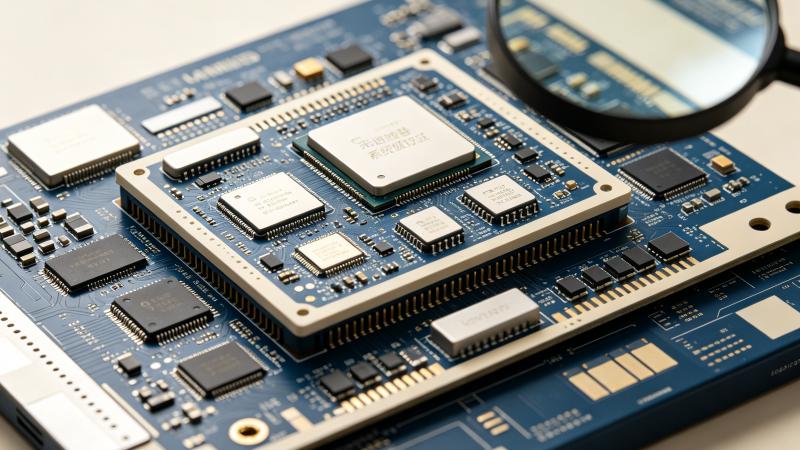
Panel Level Packaging (PLP) Technology
Panel Level Packaging (PLP) Technology An in-depth analysis [...]
Photoresist for Panel-Level Packaging | Key Material for Advanced Packaging Lithography
Photoresist for Panel-Level Packaging Photoresist for Panel-Level Packaging | Key [...]
To reach our anytime via email please fill out the form below with your request and a company representative will reply to you. To find your local CHEERSONIC representative to connect directly click your region in the contact drop down menu.
Contact CHEERSONIC For immediate assistance please contact us the corporate headquarters during business hours at 6:00 am – 22:00 pm.
Tel: 0571-87910406
- Mobile: +86 15869049660
- Email: Market2@cheersonic.com
Add: 11-13 Chuangye Road, Changkou, Fuyang, Hangzhou, Zhejiang, China
