Photoresist for Panel-Level Packaging
Photoresist for Panel-Level Packaging | Key Material for Advanced Packaging Lithography
As advanced semiconductor packaging evolves toward large-area, high-density, and low-cost heterogeneous integration, Panel-Level Packaging (PLP) has emerged as a key technological pathway to complement and optimize traditional wafer-level packaging. Unlike circular wafer packaging, PLP utilizes large rectangular panel substrates, integrating hundreds or even thousands of chip units in a single batch, thereby significantly boosting production efficiency and substrate utilization. Underlying this innovative manufacturing model, photoresist serves as an indispensable core material for micro-fabrication; it directly determines the precision, stability, and yield of critical packaging processes such as Redistribution Layer (RDL) patterning, bump formation, and dielectric layer structuring. Photoresists specifically designed for PLP differ significantly from traditional front-end wafer photoresists in terms of material properties and process requirements, as they must accommodate the unique large-format, multi-unit integration scenarios characteristic of PLP.
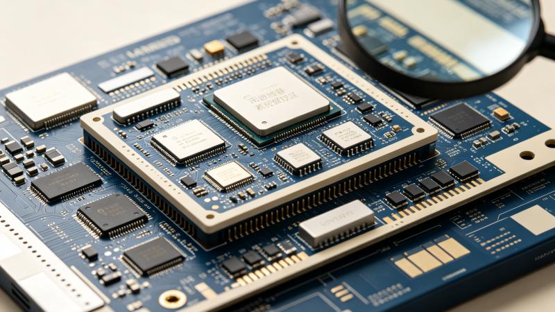
Photoresists are a class of photosensitive functional materials that undergo chemical changes upon exposure to specific wavelengths of light, enabling selective etching, protection during electroplating, and pattern transfer. Throughout the complete PLP workflow, photoresists play a vital role in multiple core manufacturing stages. Prior to RDL fabrication, photoresist forms precise mask patterns on the dielectric surface to guide the formation of ultra-fine metal circuitry. During the fabrication of micro-bumps and pads, thick-film photoresist provides high-aspect-ratio masking patterns, ensuring uniform dimensions and precise positioning of conductive structures. In subsequent stages—such as panel dicing and pre-treatment for functional testing—the photoresist acts as a protective layer, preventing damage to the packaging unit structures. Compared to standard or wafer-level photoresists, PLP photoresists prioritize large-area film uniformity, the ability to form complex micro/nano-structures, and high-temperature process stability, thereby meeting the demands of long, multi-cycle manufacturing processes involving large panels.
The most significant technical challenges in the application of PLP photoresists lie in achieving uniform large-area deposition and stable lithographic performance. Traditional wafer packaging relies on spin-coating processes capable of forming uniform thin films on small-diameter circular wafers; however, this method reveals significant limitations when applied to ultra-large rectangular panels. Spin-coating processes applied to large panels are prone to issues such as edge bead accumulation, thinning of the central film layer, and streaking defects; furthermore, they entail significant material waste, making it difficult to meet the mass production and precision requirements of panel-level packaging (PLP). Additionally, large panels are susceptible to slight warpage and thermal deformation after undergoing multiple high-temperature processing steps, imposing stricter standards on the flatness, adhesion, and stress resistance of the photoresist film.
PLP requires the precise deposition of photoresist onto large-area substrates containing hundreds or thousands of individual packaging sites. Ultrasonic coating systems can apply uniform photoresist layers over redistribution layers (RDLs), bond pads, dielectric surfaces, and patterned structures, ensuring the accuracy of the photolithography process in advanced packaging manufacturing. Ultrasonic spraying achieves stable, consistent film thickness across the entire panel, mitigating defects common to traditional coating methods—such as pooling, streaking, and edge-related irregularities. This is particularly critical for large rectangular panels, where spin-coating often results in substantial material waste and uneven film distribution.
In terms of material classification, photoresists designed for PLP primarily include positive-tone and negative-tone thick-film photoresists, as well as dry-film photoresists widely used in high-precision applications. Positive-tone photoresists offer excellent resolution, making them suitable for patterning fine RDLs with minimal linewidths and meeting the high-density interconnect requirements of AI chips and high-performance computing devices. Negative-tone thick-film photoresists can form stable, thick layers with superior resistance to electroplating, making them ideal for fabricating micro-bump arrays and patterning thick metal layers. Dry-film photoresists provide outstanding step coverage and lamination uniformity, effectively avoiding bubble defects associated with liquid photoresists and making them better suited for the large-scale mass production of PLP panels.
Beyond coating uniformity, PLP photoresists must meet various industrial reliability standards. First, they require low thermal shrinkage and low outgassing properties to prevent pattern distortion or contamination during multiple high-temperature curing cycles. Second, they must exhibit strong adhesion to diverse substrates—such as glass, organic dielectric layers, and metal bases—to prevent pattern delamination or edge lifting during the development and etching stages. At the same time, appropriate photosensitivity and a wide process window allow the material to accommodate minor parameter fluctuations during large-area panel lithography, thereby reducing yield variations between batches. These distinct performance requirements position PLP photoresists as high-barrier semiconductor materials, distinct from traditional wafer-level photoresist systems.

As the industrialization of panel-level packaging (PLP) accelerates, the pace of innovation for supporting photoresist materials is quickening. Early panel packaging efforts largely relied on modified wafer-level photoresists, which suffered from poor compatibility with large-area processes and low mass-production yields. Today, however, customized PLP photoresist formulations have achieved breakthroughs in areas such as thick-film uniformity, high-resolution patterning, and low-stress film formation. When paired with ultrasonic coating processes, these materials resolve industry challenges regarding precise photoresist deposition over large areas, effectively facilitating the large-scale adoption of fan-in and fan-out panel-level packaging.
Looking ahead, driven by demands for heterogeneous integration, chiplet packaging, and high-reliability automotive packaging, PLP technology will evolve toward larger panel sizes, finer circuitry, and higher integration densities. This places greater demands on photoresist performance, requiring capabilities such as ultra-thick uniform film formation, ultra-fine pattern resolution, and resilience in extreme environments. As a critical material determining PLP process precision, specialized photoresists—combined with advanced ultrasonic coating and lithography techniques—will continue to drive the upgrading of advanced packaging technologies, serving as a key enabler for overcoming the performance bottlenecks of traditional semiconductor packaging.
About Cheersonic
Cheersonic is the leading developer and manufacturer of ultrasonic coating systems for applying precise, thin film coatings to protect, strengthen or smooth surfaces on parts and components for the microelectronics/electronics, alternative energy, medical and industrial markets, including specialized glass applications in construction and automotive.
Our coating solutions are environmentally-friendly, efficient and highly reliable, and enable dramatic reductions in overspray, savings in raw material, water and energy usage and provide improved process repeatability, transfer efficiency, high uniformity and reduced emissions.
If you have any technical questions, customization demands, or procurement inquiries about ultrasonic atomization nozzles, feel free to contact our professional sales and technical team for detailed parameters, customized solutions, and industry application support.
Email: market2@cheersonic.com