
Microelectronic Coating
Ultrasonic coating equipment delivers high-precision thin layer deposition tailored to sophisticated microelectronic hardware and assorted electronic parts. The equipment handles a wide range of coating materials, ranging from photoresist thin layers and conductive polymer coatings to electromagnetic interference shielding layers and soldering flux films used in high-end packaging processes. These coating setups generate evenly distributed coating layers while boasting outstanding material utilization rate, strong coating bonding performance, and stable processing repeatability.
The technology relies on low-speed ultrasonic atomization to create adjustable coating solutions compatible with most solvents. It maintains steady coating quality even on intricately shaped base materials and drastically cuts raw material waste.
This coating technology fits every production stage, from laboratory research and prototype testing all the way to mass manufacturing. Its applicable scenarios cover photoresist coating for microelectronic chips, carbon nanotube, nanowire, conductive ink and other nanomaterial coating, electromagnetic shielding film processing, sensor functional coatings, MicroLED and display panel coating, as well as flip chip soldering flux application.

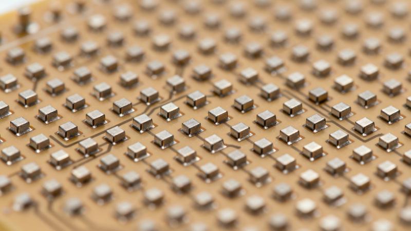
Panel Level Packaging (PLP) & Advanced Packaging
Ultrasonic spray coating enables controlled thin-layer photoresist deposition for large panel-scale semiconductor fabrication. It delivers even coverage over full panel areas, packaging positions, vias, circuit lines and intricate topographical features with high material utilization efficiency. The non-contact ultrasonic spraying process serves as a substitute for spin coating, helping manufacturers cut photoresist waste, stabilize coating uniformity, and guarantee consistent photolithography performance for enlarged panel formats.
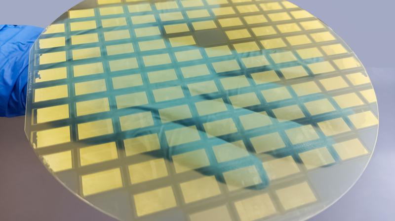
Photoresist Deposition for Microelectronics – Beyond Wafers
Ultrasonic spray coating works where spin coating fails for large flat panels, big lenses, and curved optics. It forms even photoresist layers over full surfaces and microstructures and cuts edge buildup, supporting defect-free lithography for anti-reflective and diffractive structures with no pooling or streaks.
For microfluidic chips, biosensor bases, and roll-to-roll thin films, sprayed photoresist creates solvent-resistant uniform thin films with strong adhesion and accurate patterning. High material transfer efficiency and closed-loop control reduce chemical waste while keeping steady dielectric and polymer coating thickness across all substrates.
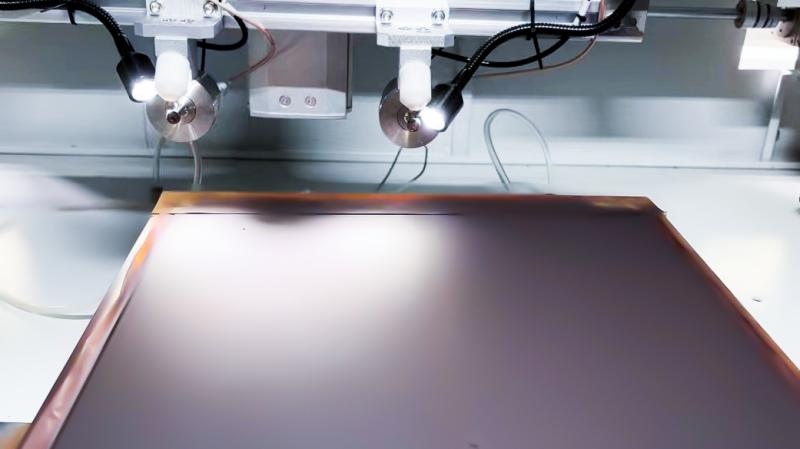
Carbon Nanotubes, Nanowires, Conductive Printing Inks and Other Nanoscale Materials
Ultrasonic atomizing spray heads evenly apply carbon nanotubes, nanowires, conductive ink mixtures and various nano dispersions to form ultra-thin functional coatings on shaped, intricate substrates.
Even particle distribution within atomized droplets eliminates nozzle blockages while boosting coating homogeneity. It stabilizes uniform conductive performance across all finished films. Such nanocoatings support manufacturing transparent conductive layers, heating films, electromagnetic interference shielding, circuit antennas and sensitive sensor coatings. Precise regulation over material output and solvent flow supports flexible production scaling, ranging from laboratory small-scale testing to large-area industrial manufacturing.

Protective Coatings for Package Level EMI Shielding
Ultrasonic spray coating stands out as a promising advanced technique for EMI shielding, capable of forming seamless, evenly distributed conductive thin layers on complex casings and component housings with accurate thickness modulation. Numerous manufacturers opt for this spraying process to fully substitute or supplement expensive traditional treatments such as metal organic chemical vapor deposition and prefabricated shielding covers. The solution cuts coating material consumption, streamlines assembly workflows and lowers finished part weight. The coating method delivers reliable bonding and stable conductive performance for both metal and polymer conductive formulations, easily adapting from laboratory research trials to continuous mass production lines.
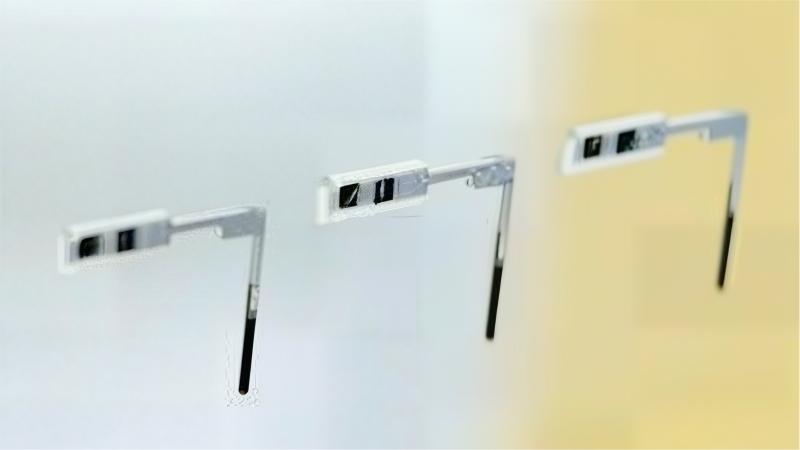
Sensor Manufacturing Coatings
Ultrasonic spray technology applies functional and protective thin films onto sensor and MEMS components, covering catalytic metal oxide coatings, conductive and dielectric films, biochemical recognition layers with enzymes, as well as hydrophobic silicone topcoats. Low-speed atomized droplets generated by ultrasonic treatment prevent damage to delicate microstructures while delivering highly controlled, even coating thickness. The resulting surface layers boost component bonding strength, electrical functionality and long-term service life, and the coating process scales smoothly from lab prototyping to large-panel and continuous roll production.

MicroLED, OLED and premium display production
MicroLED coating stays in R&D and pilot stages, with scalable thin-film encapsulation and precise flux deposition under fast development. Before LED mounting, evenly coating backplane bonding pads with thin flux is vital: flux removes oxides, improves solder wetting and bonding strength, directly affecting yield and display durability.
Ultrasonic spray technology suits this flux coating perfectly. It forms uniform ultra-thin flux films on countless micro pads with steady repeatability. Low-speed atomization and precise nozzle control avoid splashes and residues for reliable chip-pad bonds. It optimizes solder wetting, cuts contamination and raises yields better than traditional processes.
This equipment also handles polymer and organic coatings for encapsulation, planarization and getter layers. Manufacturers can tweak coating and solvent formulas easily, migrating tested recipes from R&D to pilot and initial production with high material utilization and precise film regulation.

Flip-Chip Flux Coating
Ultrasonic spraying deposits ultra-thin, even flux layers onto solder bumps and bonding pads for flip-chip processes. The coating enhances solder wetting and bonding stability in reflow steps, alongside reduced spray splatter and leftover residues. Closed-loop fluid supply paired with fine-tuned nozzle management stabilizes flux dosage, delivering highly repeatable coating results and eliminating bridging or positioning defects. The technology scales seamlessly from lab prototyping to continuous mass production, fitting high-density circuit boards and semiconductor packaging workflows.
Ultrasonic spray coating hardware adapts to mass-production microelectronics manufacturing, supporting diverse solvents and resisting nozzle blockages. The process accommodates polymer, silicone and nanomaterial coating materials. It helps electronics makers boost coating adhesion, film consistency and insulating properties for various electronic component products.
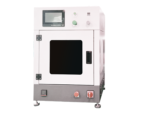
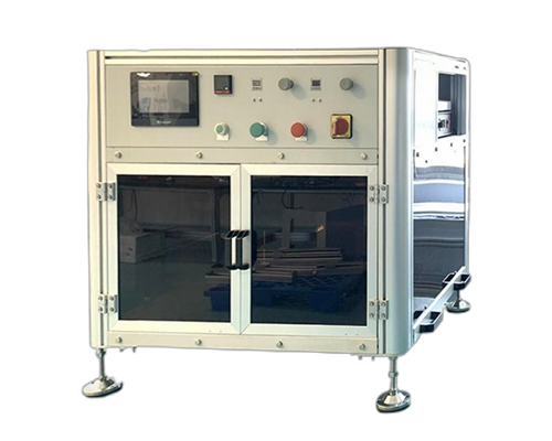
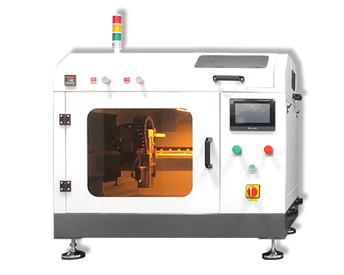
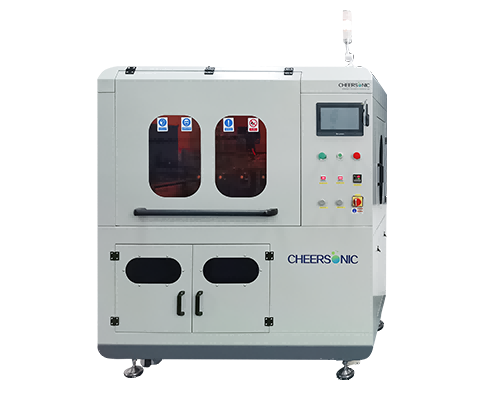
EQUIPMENT SOLUTIONS
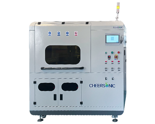
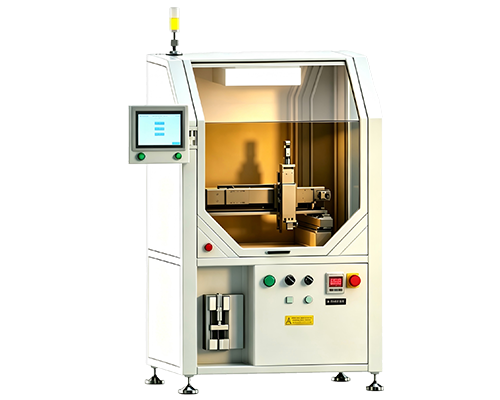
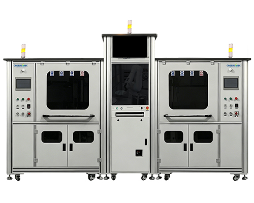
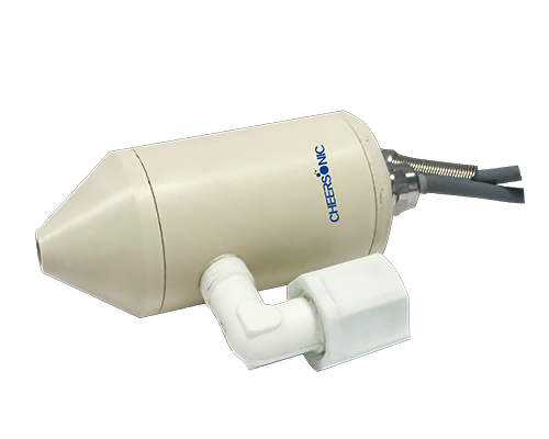
To reach our anytime via email please fill out the form below with your request and a company representative will reply to you. To find your local CHEERSONIC representative to connect directly click your region in the contact drop down menu.

Contact CHEERSONIC For immediate assistance please contact us the corporate headquarters during business hours at 6:00 am – 22:00 pm.
Tel: 0571-87910406
- Mobile: +86 13588732518
- Email: Market2@cheersonic.com
Add: 11-13 Chuangye Road, Changkou, Fuyang, Hangzhou, Zhejiang, China
