
MEMS Photoresist Spray Coating
Application analysis of ultrasonic spraying technology in MEMS photoresist spray coating
In the MEMS micro nano manufacturing process, photoresist coating is the core prerequisite of the photolithography process. The uniformity, consistency, and adhesion of the coating directly determine the etching accuracy and yield of the microstructure pattern. Traditional spin coating and dip coating processes are limited by physical principles. In the coating of complex three-dimensional microstructures, high aspect ratio grooves, and irregular substrate surfaces, there are common problems such as uneven adhesive layer thickness, incomplete sidewall coverage, and serious material waste, which are difficult to adapt to the precision manufacturing needs of high-end MEMS devices. Ultrasonic spraying technology, with its unique atomization deposition principle, breaks through the bottleneck of traditional processes and becomes the mainstream high-quality solution for MEMS photoresist spraying.
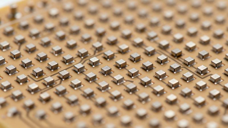
The core working principle of ultrasonic spraying machine is high-frequency ultrasonic atomization physical deposition, without high-pressure forced shearing or high-speed centrifugal stretching. The device converts electrical signals into high-frequency mechanical vibrations through piezoelectric transducers, amplifies the vibration amplitude through a variable amplitude structure, and transmits it to the nozzle end face. The photoresist liquid forms a uniform liquid film on the surface of the nozzle, which is torn into micrometer sized fine droplets with uniform particle size under the action of high-frequency standing wave vibration. The atomized droplets have concentrated particle size and good dispersion, and there is no problem of agglomeration of large particle photoresist droplets. Subsequently, guided by a controllable inert carrier gas, the droplets are steadily deposited in the form of low-speed oriented aerosols on the surface of the MEMS substrate, gradually forming a dense, uniform, and thickness controllable photoresist film. The entire physical atomization process will not damage the chemical composition and photosensitivity of the photoresist.
Compared to traditional coating processes, the technical advantages of ultrasonic spraying for MEMS photoresist coating are very prominent. The traditional spin coating process relies on centrifugal force to spread the adhesive solution, which is only suitable for flat substrates. For the common three-dimensional microstructures of MEMS such as deep grooves, micropores, and protrusions, it is prone to situations where the top adhesive layer is too thin and the bottom and sidewall adhesive layers are missing. Moreover, most of the photoresist will be thrown out by centrifugation during the process, resulting in extremely low material utilization. Ultrasonic spraying adopts a low-speed flexible deposition method, and fine droplets can uniformly cover the substrate plane, sidewalls, and deep cavity structures, perfectly adapting to the coating requirements of high aspect ratio microstructures and effectively solving the problem of coating blind spots in complex shaped substrates.
In terms of process accuracy and stability, this equipment can achieve precise control of photoresist film thickness by precisely adjusting parameters such as ultrasonic vibration frequency, spraying distance, moving speed, and gas flow rate. The film thickness error can be stably controlled within a very small range, and the coating repeatability is excellent. At the same time, ultrasonic vibration has self-cleaning characteristics, and the nozzle is not easily blocked during the spraying process, which can operate continuously and stably for a long time, greatly reducing equipment maintenance costs and process fluctuation risks. In addition, this process does not require a large amount of solvent dilution of photoresist, which reduces consumables waste and environmental pollution, while ensuring the quality of film formation after photoresist curing, significantly improving device lithography accuracy.
In industrial applications, ultrasonic spray photoresist technology is suitable for the manufacturing of various MEMS devices, covering photolithography processes for microsensors, microactuators, optical microstructures, microfluidic devices, and other products. The characteristics of its atmospheric pressure operation do not require a vacuum environment, and it has strong process adaptability. It can be compatible with substrates of different sizes and materials, which can meet the research and development of small batch precision samples and the needs of large-scale production. At the same time, this technology simplifies the complex process of traditional adhesive coating, eliminating the need for complex substrate pretreatment and adhesive solution blending processes, effectively shortening the production cycle, and reducing overall manufacturing costs.
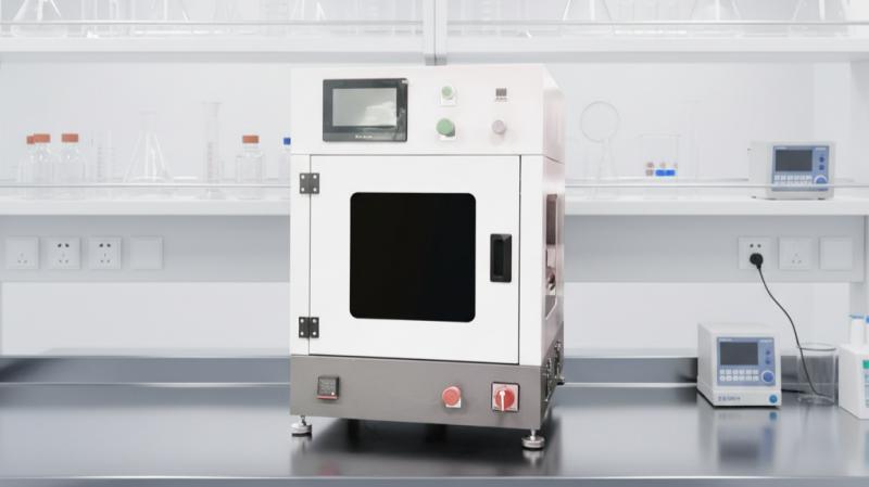
With the continuous iteration of MEMS devices towards miniaturization, high precision, and three-dimensional structuring, the requirements for fine and consistent coating of photoresist layers in photolithography technology continue to increase. Ultrasonic spraying technology, with its core advantages of high precision, high adaptability, and high material utilization, has completely made up for the shortcomings of traditional processes and has become a key technology for photoresist coating in the field of MEMS micro nano manufacturing. In the future, with the continuous optimization of process parameters and the upgrading of equipment stability, this technology will further expand its application boundaries and assist in the dual improvement of precision and efficiency in the industrialization of high-end MEMS devices.
About Cheersonic
Cheersonic is the leading developer and manufacturer of ultrasonic coating systems for applying precise, thin film coatings to protect, strengthen or smooth surfaces on parts and components for the microelectronics/electronics, alternative energy, medical and industrial markets, including specialized glass applications in construction and automotive.
Our coating solutions are environmentally-friendly, efficient and highly reliable, and enable dramatic reductions in overspray, savings in raw material, water and energy usage and provide improved process repeatability, transfer efficiency, high uniformity and reduced emissions.
If you have any technical questions, customization demands, or procurement inquiries about ultrasonic atomization nozzles, feel free to contact our professional sales and technical team for detailed parameters, customized solutions, and industry application support.
Email: market2@cheersonic.com
