
Wafer Cutting Protective Film: the Invisible Guardian of Chip Slicing Process
In the semiconductor chip manufacturing process, wafer cutting (Dicing) is a key step in dividing the entire wafer into individual chips. After the front-end processes such as photolithography, etching, and thin film deposition are completed, the wafer is still just a circular substrate covered with circuits. Only through precise slicing can the bare chips for subsequent packaging be obtained. And protective films for Dicing are the core auxiliary materials that ensure the yield of this process.
The process difficulty of wafer cutting is very prominent. A high-speed rotating cutting blade generates a huge impact force when cutting into a silicon wafer, accompanied by a large amount of cooling water flushing, which can easily cause scratches, edge breakage, and microcracks on the surface circuit of the wafer. Small silicon powder debris may also adhere to the solder pads and circuits, causing failure problems such as leakage and open circuit. The core function of the protective film is to adhere to the active surface of the wafer, firmly protect the precision circuit structure, buffer cutting stress, block debris splashing and water flow erosion, and be able to be smoothly peeled off after cutting without leaving residue on the chip surface.
This type of protective film is generally composed of a substrate layer and a pressure-sensitive adhesive layer. The substrate needs to have good tensile strength, water resistance, and dimensional stability, and there will be no tensile deformation or local tearing during the cutting process; The adhesive layer is the focus of performance design. It is necessary to maintain sufficient adhesion during the cutting stage to prevent the film from lifting and failing, and to achieve low peeling force during the film tearing process to avoid the tearing force from lifting or breaking the micro chips. According to different cutting methods, protective films also have differentiated selection. In addition to traditional blade cutting, new processes such as laser invisible cutting have raised higher standards for the heat resistance and laser transparency of protective films.
There are various methods for preparing film coatings, and the industry can achieve uniform film formation through various precision coating processes. Ultrasonic spraying can be used for thin layer preparation of protective film functional coatings, achieving precise and controllable coating thickness. Excellent uniformity of the film surface can avoid cutting force differences caused by uneven local adhesive thickness and reduce yield fluctuations. After the protective film coating is completed, it needs to be cut and tested in a clean environment to control appearance defects such as bubbles, particles, scratches, etc. Any small defects may be amplified into batch defects in the micro level precision wafer cutting process.
The performance of wafer cutting protective film directly determines the yield of chip products. If the adhesion of the protective film is insufficient, the edges will warp during cutting, and cooling water and silicon chips will directly corrode the chip circuit; Excessive adhesive residue can interfere with subsequent packaging processes such as wire bonding and plastic sealing; Poor ductility and inability to adapt to the deformation buffering requirements of thin wafers. With the development of chips towards thinning, high-density circuits, and large-sized wafers, wafers are becoming thinner and the risk of cutting edge breakage and fragmentation is further increasing. The market demand for high-performance cutting protective films continues to rise.
Semiconductor manufacturing is a closely intertwined precision engineering process, and many people focus on core processes such as photolithography and etching, but often overlook key auxiliary materials such as protective films. A small layer of film silently withstands cutting impacts, guarding the integrity of every nanoscale circuit, and is an essential “protective armor” for chips from wafers to packaging. The continuous iteration of semiconductor materials will also continue to drive the evolution of wafer cutting processes towards higher precision and lower damage.
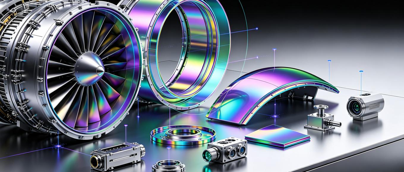
Aerospace / Aviation Coating Technology
Aerospace / Aviation Coating Technology Popularize the aerospace micro-thin [...]
To reach our anytime via email please fill out the form below with your request and a company representative will reply to you. To find your local CHEERSONIC representative to connect directly click your region in the contact drop down menu.
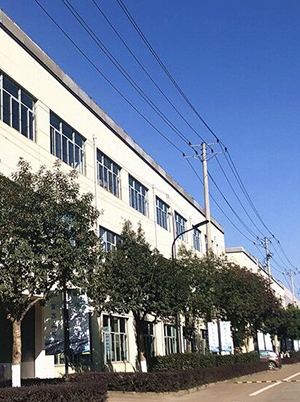
Contact CHEERSONIC For immediate assistance please contact us the corporate headquarters during business hours at 6:00 am – 22:00 pm.
Tel: 0571-87910406
- Mobile: +86 15869049660
- Email: Market2@cheersonic.com
Add: 11-13 Chuangye Road, Changkou, Fuyang, Hangzhou, Zhejiang, China
