
Ultrasonic Spray Wafer Coating Process
Ultrasonic Spray Wafer Coating Process – Photoresist Coating Systems for Photolithography Wet Process – Cheersonic
Behind the booming development of the modern electronic information industry, wafers play a crucial role as the core carrier of integrated circuits or chips. A wafer is a thin circular sheet made of high-purity silicon. As a semiconductor material, the conductivity of silicon can be precisely controlled by doping various impurities to achieve various functions. The surface of the wafer is densely covered with countless tiny electronic components, such as transistors, diodes, capacitors, etc. These components are interconnected through precise circuits, forming complex circuit patterns that perform critical tasks such as logic operations, data storage, and signal processing. During the wafer preparation process, the quality of the coating process directly affects the performance of the wafer and the quality of the chip. Ultrasonic spraying technology, with its unique advantages, has become an important innovative force in the field of wafer preparation.
Traditional wafer coating processes, such as spin coating and dip coating, gradually expose limitations when dealing with increasingly complex wafer preparation requirements. Spin coating mainly relies on centrifugal force to diffuse photoresist onto the surface of the wafer to form a thin film, which makes it difficult to achieve uniform coating on uneven or complex shaped wafers. However, immersion coating can easily lead to uneven coating thickness and material waste. In contrast, ultrasonic spraying technology provides a new solution for wafer coating.
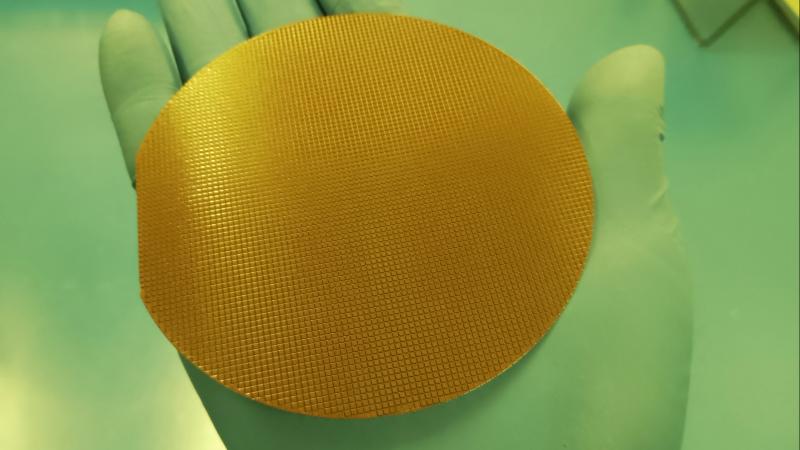
Ultrasonic spraying technology is based on high-frequency vibration, which atomizes the coating material solution into extremely small and uniform particles, and sprays them onto the wafer surface in a precisely controlled manner. This technology is widely used in wafer fabrication processes. During the photoresist coating process, ultrasonic spraying can ensure uniform coverage of the wafer surface. Even on wafers with high aspect ratio structures or complex three-dimensional shapes, coatings can achieve uniform and seamless coverage without blind spots. This provides a precise mask foundation for subsequent photolithography processes, ensuring accurate transfer of circuit patterns.
Ultrasonic spraying also performs well in the preparation of passivation and insulation layers. It can evenly coat the passivation layer and insulation material on the surface of the wafer, forming a dense and uniform coating, effectively isolating electronic components inside the wafer from external interference, and improving the stability and reliability of the wafer. For example, ultrasonic spraying plays a crucial role in preventing wafer surface oxidation, preventing impurity diffusion, and protecting circuits from electrostatic damage.
In the process of wafer metallization, ultrasonic spraying technology can achieve precise deposition of metal coatings. By precisely controlling the flow rate, coating speed, and deposition volume, a uniform thickness and strong adhesion metal layer is formed on the surface of the wafer, ensuring good electrical connection between the wafer and external circuits, and improving chip performance and yield.
The advantages of ultrasonic spraying technology are obvious. Firstly, it has extremely high uniformity. The common problems of uneven coating thickness and edge effects in traditional processes can be effectively solved by ultrasonic spraying. Its fine and uniform atomized particles can achieve micron or even nanometer level uniform coating on the wafer surface, which is crucial for wafer manufacturing that requires extremely high precision. Excellent uniformity can not only improve the consistency of chip performance, but also reduce the defect rate caused by uneven coating.
Secondly, the coating microstructure formed by ultrasonic spraying exhibits excellent encapsulation performance. The coating tightly adheres to the surface of the wafer, effectively blocking the invasion of external impurities and moisture, providing reliable protection for electronic components inside the wafer. This excellent packaging performance can significantly improve the lifespan and stability of chips even in harsh working environments.
In addition, ultrasonic spraying technology can precisely control the coating area. Through advanced layering technology and precise flow control, this technology can flexibly adjust the spraying area and coating thickness according to wafer design requirements, achieving precise local or full wafer coating. This significantly enhances the flexibility and adaptability of the process, meeting diverse wafer preparation needs.
In addition, ultrasonic spraying is not limited by the underlying material and can be applied to insulation and conductive layers. It is widely used in the preparation of complex wafer structures and can be seamlessly integrated with various wafer processing technologies, providing an integrated wafer preparation solution.
In actual production, ultrasonic spraying technology can also effectively reduce material waste. Its low-speed spray formation mode realizes the precise and controllable atomization spraying process and avoids overspray. Compared to traditional processes, this technology can save a lot of coating materials and reduce production costs. In addition, the high efficiency of this technology helps to improve production efficiency, shorten wafer preparation cycles, and bring significant economic benefits to enterprises.
With the continuous advancement of semiconductor technology, the requirements for wafer preparation processes are becoming increasingly stringent. Ultrasonic spraying technology, with its advantages of high uniformity, good encapsulation, controllable coating, and wide applicability in wafer preparation, is gradually becoming the mainstream technology in the field of wafer preparation. Its application not only promotes the innovative development of wafer preparation technology, but also provides strong support for the manufacturing of high-performance chips, and will play a more important role in the future electronic information industry.
About Cheersonic
Cheersonic is the leading developer and manufacturer of ultrasonic coating systems for applying precise, thin film coatings to protect, strengthen or smooth surfaces on parts and components for the microelectronics/electronics, alternative energy, medical and industrial markets, including specialized glass applications in construction and automotive.
Our coating solutions are environmentally-friendly, efficient and highly reliable, and enable dramatic reductions in overspray, savings in raw material, water and energy usage and provide improved process repeatability, transfer efficiency, high uniformity and reduced emissions.
Chinese Website: Cheersonic Provides Professional Coating Solutions
