
Ultrasonic Spray Coating for Semiconductor and Dielectric Layers
Ultrasonic Spray Coating Machine: Core Process Equipment for Precise Thin Film Transistor Fabrication
In the current wave of miniaturization, flexibility, and high performance transformation of electronic devices, thin film transistors (TFTs), as core components in display driving, intelligent sensing, and photovoltaic energy, directly determine the performance ceiling of end products through the precision and efficiency of their fabrication process. Ultrasonic spray coating machines, with their unique atomization deposition principle, have become key equipment for achieving precise construction of semiconductor and dielectric layers, promoting the large-scale, high-quality production of thin film transistors, and providing important support for process innovation in the electronics manufacturing field.
The Core Working Principle of Ultrasonic Spray Coating Machines: From Atomization to Precise Deposition
The core advantage of ultrasonic spray coating machines over traditional spraying equipment stems from their atomization technology based on ultrasonic vibration. During operation, high-frequency ultrasonic waves (typically in the range of 20kHz-100kHz) act on the liquid raw material within the spray head, breaking it down into uniform droplets at the micron or even nanometer scale through mechanical vibration, forming a stable “atomization cone.” This atomization method eliminates the need for high-pressure airflow, avoiding the problems of droplet splashing and particle agglomeration found in traditional high-pressure spraying. The diameter of the atomized droplets can be precisely controlled within 1-5 micrometers, with a droplet size distribution uniformity deviation of less than 10%, laying the foundation for the uniformity of the subsequently deposited film.
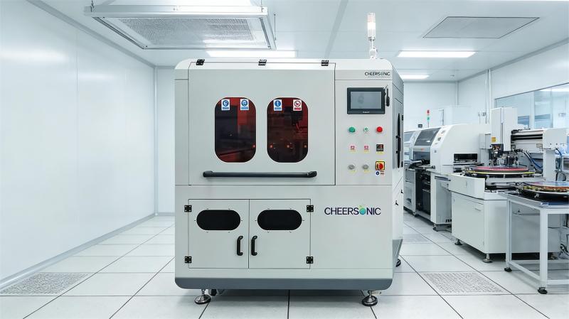
During the deposition process, the ultrasonic sprayer, through a precise motion control system (such as a servo motor-driven XYZ axis platform), enables the spray head to move at a uniform speed along a preset path. Combined with real-time adjustment of the liquid flow rate (minimum flow rate as low as 0.1 mL/h) and atomization parameters, it ensures that the droplets accurately cover the target area on the substrate surface. Simultaneously, the equipment’s temperature control system provides real-time heating to the substrate (temperature control accuracy ±1℃), allowing the droplets to dry and solidify rapidly upon contact with the substrate, reducing film thickness unevenness caused by droplet flow and further improving deposition accuracy.
Precise Deposition of Semiconductor Layers: Ensuring the Electrical Performance of Thin-Film Transistors
The semiconductor layer is the core component of thin-film transistors (TFTs) that enables current regulation. Its purity, thickness uniformity, crystallinity, and adhesion to the substrate directly affect key electrical parameters such as carrier mobility and on/off ratio. Ultrasonic spraying machines can provide suitable process solutions for different types of semiconductor materials (such as organic semiconductors, metal oxide semiconductors, and sulfide semiconductors) in semiconductor layer deposition.
Taking metal oxide semiconductor (such as IGZO) deposition as an example, the raw material is usually a metal salt solution dissolved in an organic solvent. The ultrasonic spraying machine atomizes the solution into tiny droplets by precisely controlling the atomization parameters and then evenly sprays them onto the surface of a pretreated substrate (such as glass or flexible polymer substrate). Under the heating of the substrate, the organic solvent evaporates rapidly, and the metal salt forms a dense precursor film. Subsequent annealing (typically at 200-400℃) transforms the precursor into a metal oxide semiconductor layer with good crystallinity. Throughout the process, ultrasonic spraying machines can control the thickness of the semiconductor layer to 10-50 nanometers, with a thickness deviation of less than 5% for the same batch of products, far superior to traditional spin coating processes (which typically have a deviation greater than 15%). Furthermore, due to the extremely low impact force of the atomized droplets, ultrasonic spraying machines can deposit semiconductor layers on flexible substrates without damaging them, making the fabrication of flexible thin-film transistors (TFTs) possible.
Dense Construction of the Dielectric Layer: Building a Solid Insulation Barrier for TFTs
As a key structure in TFTs that isolates the semiconductor layer from the electrodes, the dielectric layer needs to possess high insulation, low leakage current, and a dense, pinhole-free structure to prevent charge leakage between the electrodes and the semiconductor layer, ensuring stable switching performance of the transistor. In dielectric layer deposition, ultrasonic spraying machines, by optimizing process parameters, can effectively solve the problems of numerous pinholes and poor density in traditional processes.
Commonly used dielectric materials (such as silicon oxide, alumina, and organic polymer dielectric materials) mostly exist in sol-gel systems or polymer solutions. Ultrasonic spraying machines atomize these materials, forming droplets that create a continuous thin film on the substrate surface. By precisely controlling the number of sprays and the drying temperature of each layer, the thickness of the dielectric layer can be controlled in a stepwise manner (ranging from 50 nanometers to several micrometers). For example, when depositing a silicon oxide dielectric layer, ultrasonic spraying machines use multiple rounds of thin coating (5-10 nanometers thick per round) and low-temperature drying (80-120°C) to avoid the problems of uneven solvent evaporation and film cracking caused by a single thick coating. The resulting dielectric layer has a stable dielectric constant (deviation less than 3%) and a leakage current density as low as below 10⁻⁸ A/cm², meeting the insulation requirements of high-performance thin-film transistors. Simultaneously, the low-temperature deposition characteristics of ultrasonic spraying machines (with a minimum deposition temperature as low as room temperature) prevent high temperatures from damaging the performance of the deposited semiconductor layers, ensuring the compatibility of the interlayer structure.
Complete Thin-Film Transistor Fabrication: The Process Integration Value of Ultrasonic Spray Coating Machines
In the complete fabrication process of thin-film transistors (TFTs), ultrasonic spray coating machines are not standalone devices, but rather core equipment capable of efficiently integrating with processes such as substrate pretreatment, electrode fabrication, and annealing. Their process integration value is mainly reflected in three aspects:
First, broad substrate adaptability. Ultrasonic spray coating machines are compatible with both rigid substrates (glass, silicon wafers) and flexible substrates (polyimide, polyethylene terephthalate), and require no complex surface modification of the substrate. Uniform deposition on different substrate surfaces can be achieved simply by adjusting the atomization pressure and substrate temperature, providing flexible support for the fabrication of diverse TFT products (such as flexible display driving TFTs and wearable sensor TFTs).
Second, high material utilization. In traditional spin coating processes, approximately 60%-80% of the raw material is wasted due to centrifugal force being thrown off the substrate. Ultrasonic spray coating machines, through precise atomization and path control, can increase the material utilization rate to over 80%, significantly reducing the consumption of high-priced raw materials such as precious metals and rare metal oxides, thus reducing production costs. Third, it boasts strong scalability. Ultrasonic spray coating machines, through a multi-nozzle parallel design (supporting 2-8 nozzles working simultaneously), can interface with automated production lines, achieving a thin-film deposition efficiency of several square meters per hour with a stable product yield exceeding 95%. This meets the scalability requirements of thin-film transistors (TFTs) in display panels, photovoltaic modules, and other fields.
Application Prospects: Driving the Evolution of Electronic Devices Towards Higher Performance
With the rapid development of emerging fields such as flexible electronics, wearable devices, and transparent electronics, the performance requirements for TFTs are constantly increasing, further highlighting the technological advantages of ultrasonic spray coating machines. For example, in the field of flexible OLED displays, flexible TFTs fabricated using ultrasonic spray coating machines can have a bending radius as low as 5 mm. After 100,000 bending cycles, their electrical performance degradation is less than 10%, far superior to products fabricated using traditional processes. In the field of smart sensors, ultrasonic spray coating machines can precisely deposit semiconductor and dielectric layers on tiny substrates (such as the end face of a 1 mm diameter optical fiber), fabricating highly sensitive temperature and humidity sensors, expanding the application boundaries of TFTs.
In the future, with the continuous upgrading of ultrasonic spraying technology in terms of atomization precision, material compatibility, and process automation, it will not only be limited to the deposition of semiconductor and dielectric layers, but may also be further applied to the preparation of electrode materials and functional modification layers, realizing integrated spraying and molding of the entire structure of thin film transistors. This will bring more efficient, more precise, and more environmentally friendly process solutions to the electronics manufacturing field, and promote the entire industry to develop towards higher performance, lower cost, and more sustainable directions.
About Cheersonic
Cheersonic is the leading developer and manufacturer of ultrasonic coating systems for applying precise, thin film coatings to protect, strengthen or smooth surfaces on parts and components for the microelectronics/electronics, alternative energy, medical and industrial markets, including specialized glass applications in construction and automotive.
Our coating solutions are environmentally-friendly, efficient and highly reliable, and enable dramatic reductions in overspray, savings in raw material, water and energy usage and provide improved process repeatability, transfer efficiency, high uniformity and reduced emissions.
Chinese Website: Cheersonic Provides Professional Coating Solutions
