
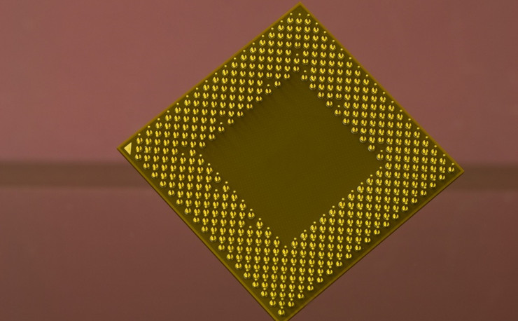
Three methods of 3D chips
Three methods of 3D chips – Ultrasonic Nozzle Spray – Cheersonic
For several years, system-on-chip developers have started breaking down their ever-larger designs into smaller chiplets and linking them together within the same package, effectively increasing silicon area among other benefits. In CPUs, these links are mostly so-called 2.5D, where chiplets are placed next to each other and connected using short, dense interconnects. As most major manufacturers have agreed on a 2.5D chiplet-to-chiplet communication standard, momentum for this integration will likely only grow.
However, to transfer really large amounts of data out as on the same chip, you need shorter, denser connections, which can only be achieved by stacking one chip on top of another. Connecting two chips face to face can mean thousands of connections per square millimeter.
It takes a lot of innovation to make it work. Engineers have to figure out how to prevent the heat from one chip in the stack from killing the other, decide which functions should go where and how they should be made, prevent the occasional bad little chip from leading to a plethora of expensive dumb systems, and deal with the attendant It’s the complexity of addressing all of these issues at once.
Here are three examples, ranging from fairly simple to confusingly complex, showing where the 3D stack is now:
AMD’s Zen 3
PCs have long offered the option to add more memory to provide faster speeds for very large applications and data-heavy work. AMD’s next-generation CPU chiplets also offer that option thanks to 3D die stacking. Of course, this isn’t an aftermarket add-on, but if you’re looking for a computer with more oomph, ordering a processor with extra-large cache memory might be the way to go.
Although both the Zen 2 and the new Zen 3 processor cores are built using the same TSMC manufacturing process — and thus have the same size transistors, interconnects, and everything else — AMD has made so many architectural changes that they make them even without additional Zen 3 can also provide an average performance improvement of 19% with the premise of the cache. One of the architectural gems is the inclusion of a set of through-silicon vias (TSVs), vertical interconnects that run directly through most of the silicon. TSV is built into Zen 3’s highest-level cache, a block of SRAM called L3, which sits in the middle of the compute chiplet and is shared among all eight of its cores.
In processors used for data-heavy workloads, the backside of the Zen 3 wafer is thinned until the TSV is exposed. A 64-megabyte SRAM chiplet is then bonded to those exposed TSVs using so-called hybrid bonding — a process similar to cold soldering copper together. The result is a dense set of connections that can be as tight as 9 microns. Finally, for structural stability and thermal conduction, a blank silicon die is attached to cover the rest of the Zen 3 CPU die.
Adding extra memory by placing it next to the CPU chip is not an option, as data takes a long time to reach the processor core. “While the L3 [cache] size has tripled, the 3D V-Cache has only added four [clock] cycles of latency — something that can only be achieved with 3D stacking,” said John Wuu, senior design engineer at AMD.
Larger caches have their place in high-end games. Using a desktop Ryzen CPU and 3D V-Cache can increase the speed of gaming at 1080p by an average of 15%. It is also suitable for more serious work, reducing the run time of difficult semiconductor design calculations by 66%.
Wuu noted that the industry’s ability to shrink SRAM is slowing compared to its ability to shrink logic. As such, you can expect future SRAM expansion packs to continue to be built using more mature manufacturing processes, while computing chips are pushed to the forefront of Moore’s Law.
Graphcore’s Bow AI processor
Even without a single transistor on a chip in the stack, 3D integration can speed up computation. Graphcore, a UK-based AI computer company, has dramatically increased its system performance simply by installing power chips on its AI processors. Adding power-supply silicon means that the combo chip, called Bow, can run faster (1.85 GHz compared to 1.35 GHz) and at a lower voltage than its predecessor. This means computers can train neural networks 40% faster and consume 16% less energy than the previous generation. Importantly, users don’t need to change their software to get this improvement.
The power management chip consists of a combination of capacitors and through silicon vias. The latter simply provides power and data to the processor chip. What really makes the difference is the capacitor. Like the bit storage components in DRAM, these capacitors are formed in deep, narrow trenches in silicon. Because these charge reservoirs are very close to the processor’s transistors, power transfer is smoothed, allowing the processor core to run faster at lower voltages. Without the power chip, the processor would have to boost its operating voltage above its nominal level to operate at 1.85 GHz, consuming more power. With a power chip, it can also hit that clock frequency and consume less power.
The manufacturing process used to make BoW is unique, but unlikely to remain that way. Most 3D stacking is done by gluing one chiplet onto another while one is still on the wafer, called a chip-on-wafer [see “AMD’s Zen 3” above]. Instead, Bow used TSMC’s wafer-to-wafer, in which whole wafers of one type are bonded to whole wafers of another type and then diced into chips. Simon Knowles, chief technology officer at Graphcore, said this is the first chip on the market to use the technology, which enables a higher density of connections between two dies than can be achieved using a chip-on-wafer process.
Although the power supply chiplets don’t have transistors, they may appear. Using the technology for power supply alone “was just the first step for us,” Knowles said. “In the near future, it will go even further.”
Intel’s Ponte Vecchio supercomputer chip
The Aurora supercomputer is designed to be one of the first high-performance computers (HPCs) in the United States to break the exaflop barrier — 1 billion high-precision floating-point calculations per second. To get the Aurora to these heights, Intel’s Ponte Vecchio packs more than 100 billion transistors on 47 pieces of silicon into a single processor. Using both 2.5D and 3D technologies, Intel squeezes 3,100 square millimeters of silicon (almost equal to four Nvidia A100 GPUs) into a 2,330 square millimeter footprint.
Intel researcher Wilfred Gomes told engineers attending the IEEE International Solid-State Circuits Conference that the processor pushes Intel’s 2D and 3D chiplet integration technology to the limit.
Each Ponte Vecchio is two mirrored chiplets bundled together using Intel’s 2.5D integration technology Co-EMIB. Co-EMIB forms a high-density interconnect bridge between two 3D chiplet stacks. The bridge itself is a small piece of silicon embedded in an encapsulated organic substrate. The density of interconnect lines on silicon can be twice as high as on organic substrates.
The Co-EMIB die also connects the high-bandwidth memory and I/O chiplets to the “foundation block,” which is the largest chiplet on the rest of the stack.
The base tile uses Intel’s 3D stacking technology, called Foveros, on which compute and cache chiplets are stacked. The technology builds a dense array of die-to-die vertical connections between two chips. These connections can be 36 microns, except for short copper pillars and solder microbumps. Signal and power enter this stack through TSVs, with fairly wide vertical interconnects running directly through most of the silicon.
Eight compute tiles, four cache tiles, and eight blank “hot” tiles for cooling from the processor are all connected to the base tile. The foundation itself provides cache memory and a network that allows any computational block to access any memory.
Needless to say, none of this is easy. It has innovated in yield management, clock circuits, thermal regulation and power delivery, Gomes said. For example, Intel engineers chose to supply the processor with a higher-than-normal voltage (1.8 volts) so that the current was low enough to simplify packaging. The circuits in the base block step down the voltage to close to 0.7 V for the compute blocks, and each compute block must have its own power domain in the base block. The key to this capability is a new type of high-efficiency inductor called a coaxial magnetic integrated inductor. Because these are built into the package substrate, the circuit actually snakes back and forth between the base block and the package before supplying voltage to the compute block.
Gomes said it took a full 14 years to go from the first petaflop supercomputer in 2008 to this year’s exaflops machine. But advanced packaging, like 3D stacking, is one of the technologies that could help shorten the next thousand-fold computing improvement to just six years, Gomes told engineers.
Original link:
https://spectrum.ieee.org/single-chip-processors-have-reached-their-limits
https://spectrum.ieee.org/amd-3d-stacking-intel-graphcore
Cheersonic is the leading developer and manufacturer of ultrasonic coating systems for applying precise, thin film coatings to protect, strengthen or smooth surfaces on parts and components for the microelectronics/electronics, alternative energy, medical and industrial markets, including specialized glass applications in construction and automotive.
