
SU-8 Photoresist
SU-8 Photoresist | MEMS/Microfluidics Dedicated Thick-Film Negative Photoresist: Performance Parameters & Application Details
For micro/nano fabrication, MEMS devices, microfluidic chips, and UV-LIGA electroforming processes, one core material is almost always indispensable—SU-8 photoresist. As a mainstream epoxy-based chemically amplified negative thick-film photoresist in the industry, it has become the preferred material for research laboratories and industrial mass production due to its core advantages such as ultra-high aspect ratio, vertical sidewalls, and stable thick-film formation.
What is SU-8 Photoresist? Core Attributes at a Glance
SU-8 photoresist was originally developed by IBM. Its name comes from Shell Epoxy, and the number 8 represents the average number of epoxy groups per molecule. It is a negative photoresist specifically designed for thick-film micro/nano fabrication.
The core photosensitive logic is simple and easy to remember: the UV-exposed area undergoes cross-linking and curing, becoming insoluble in the developer; the unexposed area can be completely cleaned and removed by the developer, resulting in extremely high forming precision. Compatible with 365nm i-line near-ultraviolet light sources, and also compatible with electron beam and X-ray lithography, it is suitable for most microfabrication equipment.
It is mainly composed of bisphenol A phenolic epoxy resin, triarylsulfonium salt photoacid generator, and a special environmentally friendly solvent ratio. The formula is stable, with strong batch consistency, meeting the needs of both scientific research experiments and industrial mass production.
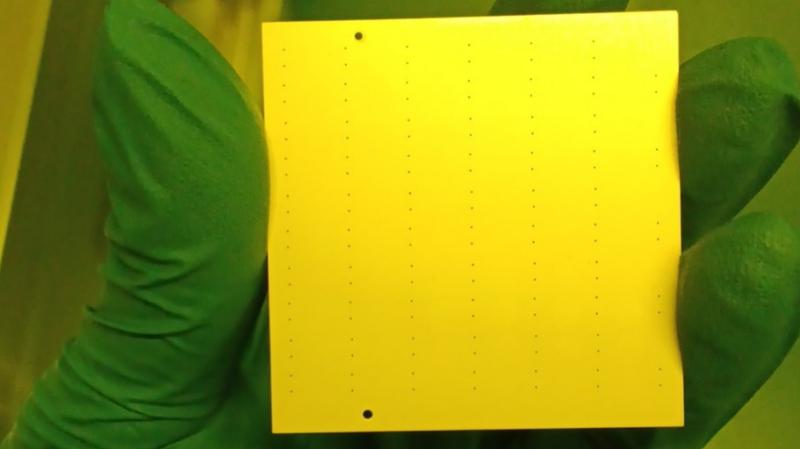
Photosensitive Imaging Principle: Chemical Amplification Process for More Stable Forming
SU-8 photoresist employs a two-step reaction imaging mechanism, which is also the key to its superiority over ordinary thick resists:
1. Ultraviolet Exposure Stage: 365nm ultraviolet light excites the photoacid generator within the resist, decomposing it to generate a super-strong protic acid. Only photosensitive energy storage is completed, without significant cross-linking reaction;
2. Post-Exposure PEB Baking Stage: Temperature rise triggers an acid-catalyzed reaction, causing the epoxy groups to undergo ring-opening polymerization, forming a dense and stable three-dimensional cross-linked structure, permanently curing and shaping the exposed area.
As a chemically amplified photoresist, the acid generated by single-photon excitation can catalyze a large number of cross-linking reactions, resulting in high sensitivity and low energy consumption, perfectly suited for the precision molding requirements of thick photoresist films.
Core Advantages: Why is SU-8 photoresist the industry’s first choice?
1. Ultra-wide film thickness adaptability, enabling ultra-thick, high aspect ratio structures: Single-layer spin-coating can stably achieve full coverage from 1μm to 250μm, while multi-layer stacking processes can exceed 500μm. Combined with SU-8 dry film products, it can achieve millimeter-thick structure molding, a core advantage that ordinary photoresists cannot replace. Simultaneously, it exhibits excellent light transmittance, with nearly vertical sidewalls in the molded form, and a conventional process aspect ratio of 15-20:1, ensuring distortion-free fine structures.
2. Extremely strong performance after curing, adaptable to multiple process scenarios: Excellent thermal stability, with a glass transition temperature exceeding 200℃, and able to withstand short-term high-temperature processes up to 250℃; resistant to acids, alkalis, and various organic solvents, suitable for demanding processes such as wet etching and metal electroforming. It possesses excellent insulation, low water absorption, and high mechanical strength, making its structure durable and resistant to deformation.
3. Dual Application Scenarios, Adaptable to Molds and Permanent Structures
It can be used as a sacrificial mold material to fabricate PDMS microfluidic master molds and metal microstructure electroforming molds, offering extremely high cost-effectiveness; it can also be used as a permanent functional structural layer, directly embedded in devices for core structures such as MEMS sensors, optical waveguides, and insulating layers.
Mainstream Model Selection Guide (Suitable for All Scenarios)
SU-8 photoresist is available in several models to precisely match processing requirements of different thicknesses and precisions. The mainstream on the market is the 2000 series, while the upgraded 3000 series focuses on low stress and high adhesion:
- 2002/2005: Thin-film models, suitable for 2-10μm fine structures, mainly used in micro-optics and high-precision micro-device processing;
- 2010/2015: Medium-thin-film models, suitable for 10-30μm structures, commonly used in conventional MEMS devices and microchannel processing;
- 2025/2035: Popular models in laboratories, suitable for 20-60μm thickness, the first choice for microfluidic PDMS master mold preparation;
- 2050/2075: Mainstream thick-film models, suitable for 50-120μm thickness, mainly used for high aspect ratio structures and metal electroforming molds;
- 2100/2150: Ultra-thick dedicated models, suitable for ultra-thick structures of 100-250μm, meeting the needs of special thick film micro-machining;
- 3000 upgraded series: Optimized internal stress, significantly improving substrate adhesion, effectively improving warpage and descaling issues, suitable for high-end precision mass production scenarios.
Standardized Process Flow (Industry-wide)
The SU-8 photoresist process is mature and highly reproducible. The general complete process is as follows: Substrate pretreatment (plasma cleaning + HMDS adhesion enhancement, eliminating descaling issues) → Precise spin coating → Stepped soft baking to remove solvent → 365nm UV exposure → Post-exposure baking and curing → PGMEA-specific development + isopropanol rinsing → Optional hard baking for reinforcement, plasma residual removal. The entire process window is stable, suitable for laboratory R&D and industrial mass production.
Process Pain Points (Objective Pitfall Avoidance Guide)
1. The cross-linked structure is extremely stable after complete curing, and cannot be removed by conventional stripping solutions. It can only be cleaned through high-temperature ashing, oxygen plasma etching, etc., making it unsuitable for conventional thin-film processes requiring subsequent desizing.
2. Ultra-thick films (>100μm) exhibit slight internal stress. Improper processing can easily lead to warping, cracking, and desizing, requiring precise control of heating and cooling rates.
3. Thick film spin coating easily produces edge beads, requiring a corresponding edge removal process. The product must also be stored in a light-proof, low-temperature, and dry environment to avoid environmental impacts on performance.
Core Application Areas
Leveraging its unique thick-film forming advantages, SU-8 photoresist has become a core consumable for micro-nano fabrication, widely used in: microfluidic chips, bioreactors, MEMS sensors and micromechanical structures, UV-LIGA metal microelectroforming, microlens arrays and optical waveguides, advanced semiconductor packaging insulating layers, micronozzles, and other precision device manufacturing. In summary, if you need to create thick films, high aspect ratios, and vertical sidewall microstructures, SU-8 photoresist is currently the best choice in terms of cost-effectiveness, stability, and versatility. All models can precisely meet the needs of scientific research experiments, pilot tests, and mass production.
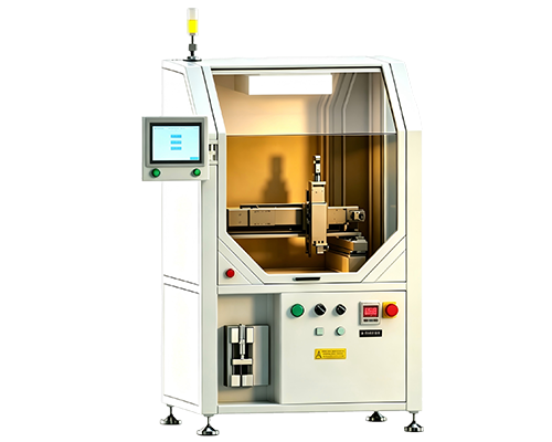
Ultrasonic spraying technology is not intended to completely replace spin coating—in conventional photolithography on standard planar substrates, spin coating remains efficient and economical. However, as the processed objects move from planar to three-dimensional, and from simple to complex, and as SU-8 needs to be precisely coated onto deep trenches, micropores, and irregular structures, ultrasonic spraying, with its superior coverage, uniformity, material utilization, and process flexibility, is becoming a key technology to overcome the bottlenecks of traditional coating methods, driving the continuous evolution of micro-nano manufacturing towards higher precision, more complex structures, and lower costs.
About Cheersonic
Cheersonic is the leading developer and manufacturer of ultrasonic coating systems for applying precise, thin film coatings to protect, strengthen or smooth surfaces on parts and components for the microelectronics/electronics, alternative energy, medical and industrial markets, including specialized glass applications in construction and automotive.
Our coating solutions are environmentally-friendly, efficient and highly reliable, and enable dramatic reductions in overspray, savings in raw material, water and energy usage and provide improved process repeatability, transfer efficiency, high uniformity and reduced emissions.
Chinese Website: Cheersonic Provides Professional Coating Solutions
