
Semiconductor Silicon Wafer Industry Barriers
Semiconductor Silicon Wafer Industry Barriers – Photoresist Spray – Cheersonic
The semiconductor wafer industry has high barriers, and the first-mover advantage and scale effect are prominent
Technical barriers: The technical parameters of semiconductor silicon wafers are highly required, and each process link needs to be accumulated for a long time. The core processes of semiconductor silicon wafers include single crystal process, slicing process, grinding process, polishing process, epitaxy process, etc. The technology has a high degree of specialization. Among them, the single crystal process is the most core technology, which determines the size, resistivity, Key technical indicators such as purity, oxygen content, dislocation, crystal defects, etc., in the single crystal growth process, need to pay attention to temperature control and pulling rate. Wafer grinding and polishing processes determine the thickness, surface flatness, surface cleanliness, surface granularity, and warpage of silicon wafers. The focus of the epitaxial process is to ensure the uniformity of the thickness of the epitaxial layer and the intra-chip uniformity of the resistivity of the epitaxial layer.
Barriers to customer certification: Chip manufacturers are cautious about introducing new suppliers and have long certification cycles. Semiconductor silicon wafers are an important raw material for chip manufacturers to produce semiconductor products. Chip manufacturers are cautious about introducing new suppliers. In order to ensure the stability and consistency of product quality, a long certification cycle is required. Usually, chip manufacturing companies will require silicon wafer suppliers to provide some silicon wafers for their trial production. After passing internal certification, the chip manufacturing company will send the products to downstream customers and obtain the approval of their customers. The supplier is certified, and finally the procurement contract is formally signed.
Capital barriers and scale barriers: The semiconductor wafer industry is a capital-intensive industry and requires a certain sales scale to be profitable. Large-scale production of semiconductor silicon wafers requires a large investment amount. For example, a key production equipment is worth tens of millions of yuan, and the investment amount of a large-scale silicon wafer production line is one billion yuan. At the same time, due to the large amount of investment in fixed assets in the early stage, semiconductor wafer companies need to form a certain scale of sales before they can make profits. The operating pressure in the early stage is relatively large, and the gross profit rate may be negative.
Talent Barriers: Semiconductor silicon wafer companies need compound talents. The R&D and production process of semiconductor silicon wafers is relatively complex, involving the intersection of solid state physics, quantum mechanics, thermodynamics, chemistry and other multidisciplinary fields. Therefore, compound talents with comprehensive professional knowledge and rich production experience are required.
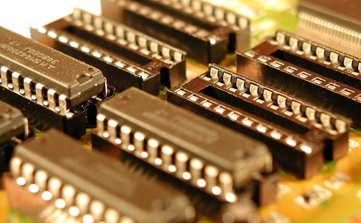
Ultrasonic spray has the advantages of precise and controllable spray flow rate, thin and uniform coating, and controllable spray range. It is very suitable for spraying electronic products and is increasingly used for research and production. Ultrasonic spray technology can be used to deposit a uniform coating on substrates of any width. Ultrasonic Spray Electronics technology enables these very thin coatings to be produced with extremely high uniformity, resulting in very accurate and repeatable results to enhance product functionality.
