
Photoresist Spraying Technology for Semiconductor Packaging
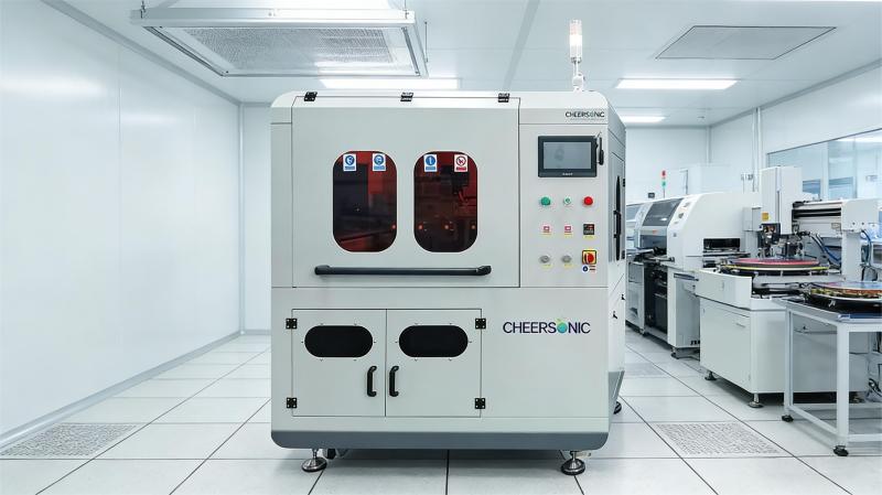
Ultrasonic photoresist spraying technology empowers advanced semiconductor packaging, helping the industry improve quality, reduce costs, and increase efficiency.
As semiconductor packaging technology rapidly iterates towards high density, high precision, and three-dimensional integration, photoresist, as a core material in advanced packaging, directly determines chip packaging precision, yield, and production costs through its coating quality, uniformity, and utilization rate. Traditional photoresist spin coating processes suffer from numerous drawbacks, including uneven coating of complex structures, significant material waste, and incomplete coverage of high aspect ratio structures, making them unsuitable for current high-end packaging process requirements. Ultrasonic photoresist spraying technology, as a new generation of precision coating process, perfectly adapts to various advanced packaging scenarios with its core advantages such as non-contact atomized spraying, uniform full-area coverage, high material utilization, and wide process adaptability, comprehensively upgrading the application effect of photoresist processes. It has now been widely implemented in various high-end semiconductor packaging production lines.
Photoresist combined with ultrasonic spraying technology comprehensively covers core semiconductor packaging processes, playing a crucial enabling role in key stages such as redistribution layer manufacturing, chip bumping, through-silicon via (TSV) insulation formation, wafer-level packaging, and temporary bonding. Specific application advantages are as follows:
I. Redistribution Layer (RDL) Manufacturing: Enabling High-Density Interconnect Forming
In cutting-edge packaging fields such as fan-out packaging (FOWLP) and 2.5D/3D stacked packaging, the redistribution layer is the core carrier for achieving high-density chip interconnects. The patterning accuracy of photoresist directly determines the stability and precision of the interconnect lines. Traditional spin coating processes are prone to problems such as uneven resist thickness, edge accumulation, and thin resist leakage on the surface of reconstructed wafers and bumped circuit structures, easily causing deviations in the circuit pattern.
Relying on ultrasonic photoresist spraying technology, micron-level uniform coating can be achieved on irregular wafer surfaces and micro-gap circuit structures through precise atomization control. The resist thickness is highly controllable and can adapt to various process requirements, including ultra-thin and thick resist layers. A stable and consistent photoresist coating can precisely define the metal pattern of the redistribution layer, guiding the precise forming of electroplating and etching processes. This significantly improves the accuracy and consistency of high-density interconnects between chips and substrates, and between chips themselves, effectively reducing short-circuit and open-circuit failure rates, and meeting the demands of ultra-high-density packaging mass production.
II. Bump Process: Ensuring High-Precision Consistency of Microbumps
Chip bumps are the core electrical connection bridges between chips and substrates, and between chips themselves. The position, size, and flatness of the bumps directly affect the chip’s conductivity and packaging reliability, requiring extremely high precision in photoresist coating. Traditional processes are prone to localized missing or uneven photoresist layers, leading to inconsistent bump sizes and positional misalignments after electroplating, affecting packaging yield.
The introduction of ultrasonic photoresist spraying technology enables uniform photoresist spraying without dead angles or deviations, precisely locking the bump forming area and providing a standardized forming template for electroplating metals such as copper and gold. This technology is perfectly suited for the fabrication of miniaturized, high-density bump arrays, completely solving the molding deviation problem of traditional processes. It comprehensively ensures the dimensional accuracy and morphological consistency of bumps, significantly improving the stability and reliability of chip electrical connections.
III. Through-Silicon Vias (TSV) Insulating Layer Formation: Overcoming Bottlenecks in 3D Packaging Processes
In 3D stacked packaging, through-silicon vias (TSVs) rely on vertical via structures to achieve vertical electrical interconnection of multi-layer chips, making them a core technology for 3D integrated packaging. TSV structures are characterized by high aspect ratios, small apertures, and vertical sidewalls. Traditional spin coating processes struggle to cover the sidewalls and bottom of the vias, easily resulting in coating gaps, adhesive layer breakage, signal crosstalk, electroplating short circuits, and other process defects. This has long been a key bottleneck restricting the mass production of 3D packaging.
Ultrasonic photoresist spraying technology perfectly solves this industry problem. Its finely atomized particles can penetrate deep into the high aspect ratio vias, achieving uniform coating with full coverage of the TSV sidewalls and bottom. The bottom coverage rate can reach over 92%, with no coating blind spots or adhesive layer breaks. The formed photoresist insulating layer effectively blocks chip signal crosstalk and provides precise patterning support for subsequent metal filling, ensuring stable electrical performance of 3D stacked packaging and facilitating the mass production of highly integrated 3D packaging.
IV. Wafer-Level Packaging (WLP) Passivation Layer Manufacturing: Enhancing Chip Protection Performance
Wafer-level packaging, with its advantages of miniaturization, high integration, and low cost, has become the mainstream packaging solution for consumer electronics and power devices. The photoresist-formed passivation layer acts as a “protective barrier” for the chip, isolating it from external environmental interference such as moisture, dust, and acid/alkali corrosion. It also provides a stable patterning base for subsequent electroplating and etching processes, requiring the photoresist layer to be complete, uniform, and have strong adhesion.
Using ultrasonic photoresist spraying technology, a uniform, dense, and stable photoresist passivation layer can be formed on the entire wafer surface. The coating adhesion and flatness far exceed those of traditional processes, making it fully adaptable to various wafer substrates and complex wafer structures. It provides long-term protection for the core circuitry of the chip, preventing device failure caused by external environmental factors, and also provides a stable process foundation for subsequent manufacturing processes, significantly improving the yield and lifespan of wafer-level packaging.
V. Temporary Bonding and Debonding Processes: Adaptable to Ultra-Thin Wafer Precision Machining
In complex packaging processes such as ultra-thin wafer thinning and fine etching, photoresist can serve as a high-quality temporary bonding material, achieving a stable bond between the wafer and the substrate. This ensures that the wafer does not shift or break during precision machining, and can be quickly and non-destructively removed through a debonding process after the process is complete.
Using ultrasonic photoresist spraying technology for bonding layer coating enables ultra-thin, uniform, and bubble-free adhesive layer formation. The wafer and substrate adhere tightly and have uniform stress, effectively avoiding warping and breakage issues in ultra-thin wafer processing. Simultaneously, the adhesive layer exhibits stable performance, is resistant to high temperatures and process corrosion, is suitable for multiple complex processing steps, and leaves no residue after debonding without damaging the wafer substrate, significantly improving the processing adaptability and process stability of ultra-thin and irregularly shaped wafers. Core Technological Advantages and Industrial Value: Advanced semiconductor packaging places stringent demands on photoresist resolution, corrosion resistance, heat resistance, adhesion, and coating uniformity. Ultrasonic photoresist spraying technology not only fully leverages the superior performance of photoresist itself but also achieves a comprehensive upgrade from the process perspective: compared to traditional spin coating, this technology increases photoresist material utilization by 30%-50%, significantly reducing raw material costs; non-contact spraying eliminates mechanical stress, preventing wafer damage; it can flexibly adapt to various complex structures such as planar surfaces, deep trenches, and high aspect ratio vias, exhibiting extremely strong process compatibility and covering all scenarios from conventional packaging to advanced processes at 7nm and below, and power device packaging.
Currently, ultrasonic photoresist spraying technology has become a core breakthrough for upgrading advanced packaging processes, effectively solving many pain points of traditional coating processes. It combines four core advantages: high precision, high yield, low cost, and high adaptability, providing strong technical support for the industrialization of semiconductor packaging towards higher integration, higher precision, and lower cost. It is the mainstream preferred process for future high-end packaging mass production.
About Cheersonic
Cheersonic is the leading developer and manufacturer of ultrasonic coating systems for applying precise, thin film coatings to protect, strengthen or smooth surfaces on parts and components for the microelectronics/electronics, alternative energy, medical and industrial markets, including specialized glass applications in construction and automotive.
Our coating solutions are environmentally-friendly, efficient and highly reliable, and enable dramatic reductions in overspray, savings in raw material, water and energy usage and provide improved process repeatability, transfer efficiency, high uniformity and reduced emissions.
Chinese Website: Cheersonic Provides Professional Coating Solutions
