
Photoresist Coating Process Technology
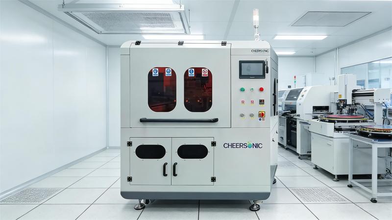
Photoresist Coating Process Technology – Photoresist Coating Systems – Cheersonic
In the fields of semiconductors, micro/nano fabrication, MEMS devices, and flexible electronics manufacturing, photoresist coating is a core pre-process in photolithography. The uniformity of the coating, the consistency of film thickness, and the surface smoothness directly determine the pattern accuracy and yield of subsequent exposure, development, and etching. Traditional photoresist coating processes mainly include spin coating, blade coating, and dip coating, each with its own advantages and disadvantages, suitable for different substrates and process requirements. However, in coating scenarios involving irregular curved surfaces, deep holes and cavities, large-size substrates, flexible films, and microstructure substrates, problems such as uneven thickness, incomplete coating at edges and corners, significant waste of resist, and the easy formation of pinholes and ripples in the film exist, making it difficult to meet the production requirements of high-precision and complex devices.
To overcome the limitations of traditional coating processes, ultrasonic spraying of photoresist has gradually become a key coating technology in high-end micro/nano manufacturing, widely used in cutting-edge fields such as precision semiconductor packaging, microfluidic chips, optical devices, and flexible circuit boards. This process relies on the principle of ultrasonic atomization. High-frequency ultrasonic vibrations uniformly atomize liquid photoresist into micron-sized droplets. Through precise inert gas flow guidance, the atomized photoresist is evenly and gently deposited onto the substrate surface, achieving full coverage of the photoresist film. This is completely different from the traditional centrifugal forming of spin coating and the contact forming of blade coating.
Ultrasonic photoresist spraying offers many unique advantages. Firstly, it provides exceptional coating uniformity. The atomized photoresist droplets have a uniform and controllable particle size, allowing for precise control of film thickness. Thickness errors can be kept within a very small range, eliminating the edge-thickness and center-thinness issues common in spin coating. It perfectly adapts to complex substrate surfaces such as planes, curved surfaces, uneven microstructures, and deep trenches and holes, achieving uniform coating without dead angles. Secondly, it boasts extremely high material utilization. Traditional spin coating processes have a photoresist utilization rate of only 5%~10%, with most of the photoresist being thrown away from the substrate by centrifugal force. Ultrasonic spraying, however, eliminates material splashing and waste, achieving a photoresist utilization rate of over 90%, significantly reducing the consumable costs of high-end photoresists. Meanwhile, this process is a non-contact coating method. During spraying, the nozzle does not come into contact with the substrate, preventing damage such as squeezing, scratches, or deformation to flexible substrates and precision microstructures. It is suitable for processing ultra-thin flexible substrates, precision chips, and fragile optical substrates. Furthermore, the process is highly adjustable. By adjusting parameters such as ultrasonic frequency, spraying distance, moving speed, and resist flow rate, photoresist films with thicknesses ranging from tens of nanometers to tens of micrometers can be flexibly prepared, adapting to various process requirements from high-precision micro-patterning to thick-film photoresist.
Compared to traditional processes, ultrasonic spraying of photoresist also features high-quality films. The atomized droplets are gently deposited, resulting in a dense and uniform film free of defects such as pinholes, bubbles, and ripples. The film adhesion is excellent, effectively improving the integrity and resolution of subsequent photolithography patterns. Moreover, the entire process is conducted at low temperatures without high-speed mechanical movement, eliminating static electricity and mechanical stress. It is suitable for the production processes of sensitive semiconductor devices, exhibiting strong compatibility and adaptability to various mainstream photoresists, including positive, negative, thick, and thin films.
Currently, ultrasonic spraying of photoresist has gradually replaced some traditional coating processes, becoming the preferred solution for irregular structures, large-size substrates, flexible electronics, and high-precision micro-nano processing scenarios. It effectively solves the pain points of traditional photoresist coating processes and plays an important role in improving product processing accuracy, reducing production costs, and expanding the application scenarios of photolithography. It is one of the important development directions of advanced photolithography manufacturing processes.
About Cheersonic
Cheersonic is the leading developer and manufacturer of ultrasonic coating systems for applying precise, thin film coatings to protect, strengthen or smooth surfaces on parts and components for the microelectronics/electronics, alternative energy, medical and industrial markets, including specialized glass applications in construction and automotive.
Our coating solutions are environmentally-friendly, efficient and highly reliable, and enable dramatic reductions in overspray, savings in raw material, water and energy usage and provide improved process repeatability, transfer efficiency, high uniformity and reduced emissions.
Chinese Website: Cheersonic Provides Professional Coating Solutions
