
Photoresist Classification
Photoresist Classification – Spray Polyimide Photoresist – Cheersonic
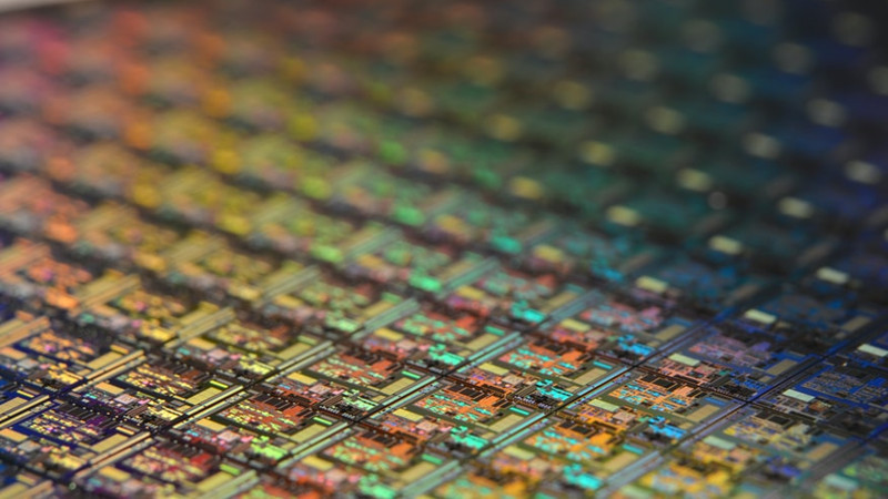
Photoresist, also known as photoresist, is a mixed liquid that is sensitive to light. Its components include: photoinitiators (including photosensitizers, photoacid generators), photoresist resins, monomers, solvents and other additives. The photoresist can transfer the required fine pattern from the photomask (mask) to the substrate to be processed through photochemical reaction and photolithography processes such as exposure and development. Depending on the usage scenario, the substrate to be processed here may be integrated circuit material, display panel material or printed circuit board. This article mainly introduces the types of photoresists from different directions.
In the flat panel display industry: the main photoresists used are color and black photoresists, LCD touch screen photoresists, TFT-LCD positive photoresists, etc. In the production process of photolithography and etching, photoresist is coated on the surface of the crystal film, and the pattern on the mask (mask) is transferred to the film after exposure, development and etching to form a pattern corresponding to the mask. geometric figures.
In the PCB industry: the main photoresists used are dry film photoresist, wet film photoresist, photosensitive solder resist ink, etc. The dry film is pasted on the treated copper-clad plate with a special film for exposure and development; the wet-film and photoimageable solder resist inks are coated on the copper-clad plate, and then exposed and developed after drying. Dry film and wet film have their own advantages. Generally speaking, the resolution of wet film photoresist is higher than that of dry film, and the price is lower. Part of the market of dry film photoresist is being replaced.
In the semiconductor integrated circuit manufacturing industry; g-line photoresist, i-line photoresist, KrF photoresist, ArF photoresist, etc. are mainly used. In the manufacturing process of large-scale integrated circuits, more than ten photolithography operations are generally performed on silicon wafers. In each photolithography and etching process, the photoresist must pass through pre-baking, gluing, pre-baking, alignment, exposure, post-baking, development and etching, etc. The graphics are transferred to the silicon wafer.
Photoresist is an important material for integrated circuit manufacturing: the quality and performance of photoresist are the key factors affecting the performance, yield and reliability of integrated circuits. The cost of the photolithography process is about 35% of the entire chip manufacturing process, and the time-consuming process accounts for about 40%-50% of the entire chip process. Photoresist materials account for about 4% of the total cost of IC manufacturing materials, and the market is huge. Therefore, photoresist is the core material of semiconductor integrated circuit manufacturing.
Classification by display effect: photoresist can be divided into positive photoresist and negative photoresist. The pattern formed when the negative photoresist is developed is the opposite of the mask (mask); the pattern formed by the positive photoresist is the same as the mask. The production process of the two is basically the same, the difference is that the main raw materials are different.
According to chemical structure classification: photoresist can be divided into photopolymerization type, photodecomposition type, photocrosslinking type and chemical amplification type. The photopolymerizable photoresist uses ethylenic monomers, which generate free radicals under the action of light, which further initiates the polymerization of the monomers, and finally generates polymers; the photodecomposable photoresists use materials containing diazoquinones (DQN) as The sensitizer, which undergoes a photolysis reaction after being illuminated, can be made into a positive photoresist; the photocrosslinking photoresist uses polyvinyl alcohol laurate as a photosensitive material, and under the action of light, a photoresist is formed. Insoluble network structure, and play a role in resist, can be made into negative photoresist. After the semiconductor integrated circuit lithography technology began to use the deep ultraviolet (DUV) light source, the chemical amplification (CAR) technology gradually became the mainstream of the industry application.
In chemically amplified photoresist technology, the resin is polyethylene protected by chemical groups and thus difficult to dissolve. Chemically amplified photoresists use photoacids (PAGs) as photoinitiators. (Schematic diagram of the photocrosslinking reaction) When the photoresist is exposed, the photoacid agent (PAG) in the exposed area will generate an acid. This acid acts as a catalyst during the post-heat bake process and will remove the resin’s protecting groups so that the resin becomes more soluble. The chemically amplified photoresist has 10 times the exposure speed of DQN photoresist, and has good optical sensitivity to deep ultraviolet light sources, as well as high contrast and high resolution.
According to exposure wavelength classification: photoresist can be divided into ultraviolet photoresist (300~450nm), deep ultraviolet photoresist (160~280nm), extreme ultraviolet photoresist (EUV, 13.5nm), electron beam photoresist, Ion beam photoresist, X-ray photoresist, etc. Photoresists with different exposure wavelengths have different limit resolutions for photolithography. Generally speaking, the shorter the wavelength, the better the processing resolution when using the same process method.
Ultrasonic spray has the advantages of precise and controllable spray flow rate, thin and uniform coating, and controllable spray range. It is very suitable for spraying electronic products and is increasingly used for research and production. Ultrasonic spray technology can be used to deposit a uniform coating on substrates of any width. Ultrasonic Spray Electronics technology enables these very thin coatings to be produced with extremely high uniformity, resulting in very accurate and repeatable results to enhance product functionality.
