
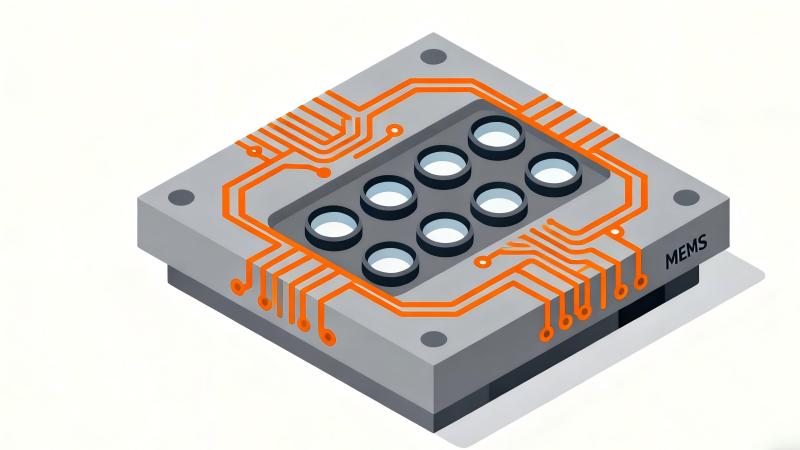
Introduction to MEMS Micromirrors
Micro Electro Mechanical Systems (MEMS) technology is a manufacturing technique for microstructures at the nanometer to micrometer scale. It originates from the semiconductor and microelectronics process system, integrating various modern processing methods such as photolithography, epitaxy, thin film deposition, oxidation, diffusion, ion implantation, sputtering, evaporation, etching, slicing, and packaging. The core is to manufacture complex three-dimensional shapes through microfabrication, essentially achieving the miniaturization integration of electrical and mechanical systems. This process not only widely supports the research and manufacturing of various microdevices, but also promotes breakthroughs in the field of technology towards miniaturization, integration, and intelligence, bringing transformative effects to multiple industries.
Technical Advantage
As a representative application result of this technology, microelectromechanical system micromirrors (MEMS micromirrors) have demonstrated outstanding technological advantages in multiple high-tech fields:
1. High precision and high-speed response light control
- High precision scanning: With the support of precise mechanical structure design and electronic control system, micro mirrors can achieve high-precision scanning of light, with scanning positioning errors controlled within a small range, meeting the requirements of precision optical control.
- Fast dynamic response: The mechanical response speed of the micro mirror is extremely fast, and it can adjust the direction and angle of light propagation in milliseconds or even microseconds, fully adapting to scenarios with strict response time requirements such as high-speed scanning and dynamic measurement.
2. Miniaturization, lightweighting, and low power consumption characteristics
- Compact size: With the high integration feature of microfabrication technology, the overall structure of the micro mirror is highly compact, occupying much less space than traditional optical adjustment components.
- Lightweight: Due to its streamlined size, its weight has been significantly reduced, which not only reduces the load on the equipment support structure, but also further enhances the operational stability and long-term reliability of the entire system.
- Low power operation: With low energy consumption during operation, it can effectively extend the device’s battery life and reduce energy costs during long-term use.
3. Coverage of diverse application scenarios
MEMS micro mirrors have a wide range of applications and can be used as core components to meet the needs of multiple fields
- In the field of LiDAR, it is a key component in scenarios such as autonomous driving, drone navigation, and robot environment perception, responsible for the emission and reception control of light;
- In the field of optical imaging, it is widely used in 3D cameras, AR/VR headsets, micro projectors, and medical imaging devices. By accurately adjusting the angle and position of the micro mirror, fine control of light is achieved, improving imaging clarity and stability;
- In the field of communication and display, it can be used for precision tracking mirrors, optical switches, high-definition display devices, vehicle head up displays (HUDs) and other products in space laser communication and fiber optic communication, playing a role in optical signal regulation.
4. Easy integration and large-scale production capacity
- High compatibility integration: It can be integrated with microcircuit units on a single chip to build a complete micro functional system. This highly integrated feature not only simplifies the overall design and manufacturing process of the equipment, but also reduces the connection loss between components, thereby improving the comprehensive performance and operational reliability of the system.
- Large scale mass production: With standardized microfabrication processes, hundreds or even thousands of structurally consistent micro mirror devices can be simultaneously manufactured on a single wafer, achieving efficient mass production. This production mode can not only quickly meet the demand for market scale, but also reduce unit product costs and improve cost-effectiveness through mass production effects.
In summary, MEMS micro mirrors play an increasingly prominent role in modern technology due to their multiple advantages such as high-precision scanning, fast response, miniaturized design, low-power operation, wide application adaptability, easy integration, and mass production. They have become an important support for promoting innovative development in optical technology, intelligent devices, and other fields.
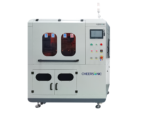
To meet the photoresist coating requirements of MEMS wafers and substrates with different morphologies, ultrasonic spraying technology has become a key process with its unique advantages. It atomizes photoresist into micrometer sized uniform droplets through ultrasonic vibration, and achieves precise coating with a precision motion control system.
For the micro nano structures of MEMS wafers, such as high aspect ratio grooves and convex arrays, this technology can solve the shadow effect problem of traditional spraying by adjusting the ultrasonic frequency (usually 20-180kHz) and atomization pressure to allow droplets to penetrate the microstructure gaps, forming a bubble free and uniformly thick (within ± 5%) coating. For irregular substrates (such as curved surfaces and stepped substrates), the non-contact spraying method can adapt to complex shapes. By dynamically adjusting the nozzle distance and movement path, the consistency of coating in different areas is ensured, meeting the strict requirements of photolithography process for the flatness of the adhesive layer.
In addition, the material utilization rate of this technology is over 80%, far exceeding traditional air spraying (30% -50%), and the droplet size is controllable (1-50 μ m), providing reliable support for high-precision manufacturing of MEMS devices and multi morphology substrates.
About Cheersonic
Cheersonic is the leading developer and manufacturer of ultrasonic coating systems for applying precise, thin film coatings to protect, strengthen or smooth surfaces on parts and components for the microelectronics/electronics, alternative energy, medical and industrial markets, including specialized glass applications in construction and automotive.
Our coating solutions are environmentally-friendly, efficient and highly reliable, and enable dramatic reductions in overspray, savings in raw material, water and energy usage and provide improved process repeatability, transfer efficiency, high uniformity and reduced emissions.
Chinese Website: Cheersonic Provides Professional Coating Solutions
