
How a lithography machine works
How A Lithography Machine Works – Lithography Coating System – Cheersonic
In the entire chip manufacturing process, the implementation of almost every process is inseparable from the technology of photolithography. Lithography is also the most critical technology for manufacturing chips, accounting for more than 35% of the cost of chip manufacturing.
When the chip completes the IC design, it is necessary to entrust the foundry to carry out the chip manufacturing and packaging.
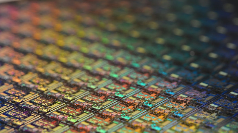
In chip manufacturing, wafers are indispensable. Silicon rods are purified from silicon dioxide (SiO2) ore, such as quartz sand, by a series of chemical and physical smelting methods, and then cut into circular monocrystalline silicon wafers. wafer.
Wafers are the basis for making all kinds of computer chips. We can compare chip manufacturing to building a house with building blocks, and by stacking layer by layer, we can complete our desired shape (that is, all kinds of chips). However, if there is no good foundation, the built house will be crooked and unsatisfactory. In order to make a perfect house, a stable base plate is required. For chip manufacturing, this substrate is the wafer.
Lithography is a precise microfabrication technology. Conventional lithography technology uses ultraviolet light with a wavelength of 2000-4500 angstroms as the image information carrier, and uses the photoresist lithography etchant as the intermediate (image recording) medium to realize the transformation, transfer and processing of the image, and finally transmit the image information. A process on a wafer (mainly a silicon wafer) or a dielectric layer.
Photolithography technology is to make the circuits and functional areas required for chip fabrication. Simply put, the circuits and functional areas designed by chip designers are “printed” into the wafer, similar to taking pictures with a camera. The photos taken by the camera are printed on the negative, and photolithography engraves not the photos, but the circuit diagrams and other electronic components.
It’s like an empty brain. The instructions are put in through lithography technology, then the brain can work, and the circuit diagram and other electronic components are the instructions designed by the chip designer.
Lithography includes two main aspects of photocopying and etching processes:
1. Optical copying process: The device or circuit pattern prefabricated on the reticle is accurately transferred to the photoresist thin layer pre-coated on the surface of the wafer or on the dielectric layer through the exposure system according to the required position.
2. Etching process: Remove the unmasked wafer surface or dielectric layer of the resist thin layer by chemical or physical methods, so as to obtain a pattern that is completely consistent with the resist thin layer pattern on the wafer surface or dielectric layer. The functional layers of the integrated circuit are three-dimensionally overlapped, so the photolithography process is always repeated many times. For example, a large-scale integrated circuit needs about 10 lithography times to complete all the transfer of each layer pattern.
The photocopying technology is the lithography machine, and the etching process is the etching machine.
Under the principle of lithography technology, people have manufactured a lithography machine. The lithography machine transmits the light beam through a mask with a circuit diagram through a series of light source energy and shape control methods, and compensates for various optical errors through the objective lens. The circuit diagram is scaled down and then mapped onto the wafer. Different lithography machines have different imaging ratios, ranging from 5:1 to 4:1. It is then developed using chemical methods, resulting in a circuit diagram (ie, a chip) etched on the wafer.
The general lithography process needs to go through such processes as cleaning and drying the surface of the silicon wafer, priming, spin-coating photoresist, soft baking, alignment exposure, post-baking, developing, hard baking, and laser etching. After one photolithography, the chip can continue to be glued and exposed. The more complex the chip, the more layers of the circuit map, and the more precise the exposure control process is required. Advanced chips now have more than 30 layers.
It can be said that lithography determines the precision of semiconductor circuits, as well as the power consumption and performance of chips. Related equipment requires the most advanced technologies in the fields of integrated materials, optics, and electromechanics.
