
Maskless Lithography
Maskless Lithography – Semiconductor Coating – Cheersonic
Masks are complicated to make, have a long cycle and are expensive. Once completed, they cannot be modified. While masks help the rapid evolution of the industry, these defects also severely limit the development of the industry. In order to achieve a more flexible lithography process, the industry has begun to study replacing physical masks with other things, or even processing without masks at all. Such a method is called “maskless lithography”.
In the field of pan-semiconductor, lithography technology is mainly divided into mask lithography and direct writing lithography according to whether a mask is used or not.
Direct-write lithography, also known as maskless lithography, refers to the focused projection of a computer-controlled high-precision beam onto the surface of a substrate coated with a photosensitive material, without the need for a mask for direct scanning exposure.
Direct writing lithography can be roughly further divided into two main types according to different radiation sources: one is charged particle-based direct writing lithography (CPML), including electron beam direct writing, ion beam direct writing, etc.; the other is Optical-based direct-write lithography (OML), including interference lithography, laser direct-write lithography, and spatial light modulator-based lithography.
Electron beam direct writing lithography: A technique that uses electron beams to draw patterns on samples coated with electron beam glue.
The advantage of this technology is that the wavelength of the high-energy electrons in the electron beam is extremely short, so the resolution is high, and the microstructures at the nanometer level can be processed. At the same time, it uses the direct writing method to expose the graphics, and the processing method is very flexible.
The disadvantages are: in stereo light, the etching depth is related to various factors in the process, and it is difficult to precisely control the etching depth; the structure of equipment such as electron beam emitters is complex and expensive; the technology uses single-point direct writing This method requires long-term accumulation of high-energy electrons for exposure in the depth direction, so it is not suitable for mass and large-area production.
Ion beam direct writing lithography technology: Due to the large mass of ions, materials and devices can be etched, deposited, ion implanted and other micro-nano processing after accelerated aggregation, which is called concentrated ion beam direct writing technology.
In the ion beam direct writing processing system, the ion beam from the liquid metal ion source is concentrated on the surface of the sample after being processed by acceleration, mass analysis, and shaping. The high-energy ion beam is concentrated on the surface of the sample and bombarded point by point, and the specific pattern can be processed by the computer-controlled beam scanner and blanking components, without the need for a mask.
In contrast, ions are much more massive than electrons, which can largely overcome the scattering problem of electron beams in resists. However, the mass of the field ions is large, resulting in a small penetration depth in the photoresist; the energy of the ion beam formed by the field ions is relatively scattered, and the focal depth is not large, resulting in low resolution; in addition, the equipment of ion beam lithography is complex, This leads to high production costs and insufficient development potential.
Interference lithography: Laser interference lithography refers to the use of light interference and diffraction characteristics to control the light intensity distribution in the interference field through a specific beam combination, and record it with a photosensitive material to generate a lithography pattern.
Laser interference lithography can be divided into two-beam, three-beam, four-beam and five-beam interference lithography according to the number of beams involved in the interference.
The interference lithography process is simple and low-cost, and can easily expose large areas with high resolution. The disadvantage is that it can only be used for exposure of periodic patterns. Periodic patterns are synthesized from a limited number of sinusoidal series, which are only approximate results, so the continued improvement of resolution is limited.
Based on spatial light modulator lithography technology (SLM maskless lithography technology): use programmable SLM devices to directly modulate the illumination beam to form different patterns and directly project them on the substrate to complete the exposure, which is equivalent to the physical Reticle digitization, known as SLM-based digital lithography.
SLM is a micro-device that can modulate the spatial distribution of light, and is composed of many tiny units arranged in a linear or square matrix. These units are controlled by computer programming to easily digitize the pattern mask, and change the shape of the mask through programming flexibility, replacing the “physical mask” used in traditional lithography, thereby avoiding the traditional lithography system mask manufacturing. Complex and expensive, poor flexibility and other issues.
In the industrial production of pan-semiconductor, the lithography accuracy (minimum line width) required by the market segment of direct-write lithography and mask lithography is significantly different.
It is understood that in the lithography application field with substrate warpage and substrate deformation, the self-adaptive adjustment ability of direct writing lithography makes it have the advantages of high yield and good consistency, and also has the advantages that projection lithography does not have. High flexibility, low cost and shortened process flow and other technical characteristics, mainly used in mask manufacturing, IC back-end packaging, low-generation FPD manufacturing, and some low-end IC front-end manufacturing.
However, the direct-write lithography technology is also limited by factors such as production efficiency and lithography accuracy, and currently cannot meet the needs of large-scale manufacturing in the pan-semiconductor industry. On the one hand, it is because the production efficiency of charged particle direct writing lithography technology is low, and it will produce a relatively serious proximity effect in large-scale production, which seriously affects the resolution and accuracy of graphics; on the other hand, laser direct writing lithography technology. Limited by the wavelength of the laser, the lithography accuracy is not as good as that of the charged particle direct writing lithography technology such as electron beam and ion beam, and it cannot meet the needs of high-end semiconductor device manufacturing.
The current industry consensus on maskless lithography is that it is a potential solution to reduce the soaring rise of photomasks and is a promising candidate for lithography. But it is still in an early stage of development, and there are still many technical problems to be solved. It may be just a subdivision of lithography technology in the near future and cannot replace the mainstream DUV and EUV lithography technology, but its lower cost will make it continue to attract attention in the future.
Original L Chenguang Semiconductor Industry Observation
The ultrasonic coating system can use advanced layering technology to precisely control the flow rate, coating speed and deposition amount. Low-speed spray forming defines an atomizing spray as a precise, controllable pattern, avoiding excessive spraying when producing very thin and uniform layers. It turns out that direct spraying using ultrasonic technology is a reliable and effective way to deposit photoresist on 3D microstructures, thereby reducing equipment failures caused by excessive metal exposure to etchant.
Ultrasonic spray systems have proven to be suitable for a variety of applications that require uniform, repeatable photoresist or polyimide film coatings. Cheersonic’s coating system can control thicknesses from sub-micron to more than 100 microns, and can coat any shape or size. It is a feasible alternative to other coating technologies such as spin coating and traditional spray coating.
Cheersonic’s non-blocking ultrasonic coating technology is known for its ultra-thin micron-layer coatings of functional and protective materials. The ultrasonic vibration of the nozzle effectively dispersed the particles in the suspension and produced a very uniform particle dispersion in the film layer, while the conductive particles did not settle out of the suspension.
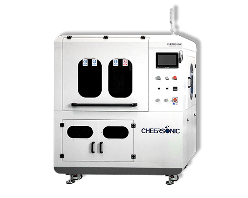
Cheersonic is the leading developer and manufacturer of ultrasonic coating systems for applying precise, thin film coatings to protect, strengthen or smooth surfaces on parts and components for the microelectronics/electronics, alternative energy, medical and industrial markets, including specialized glass applications in construction and automotive.
