
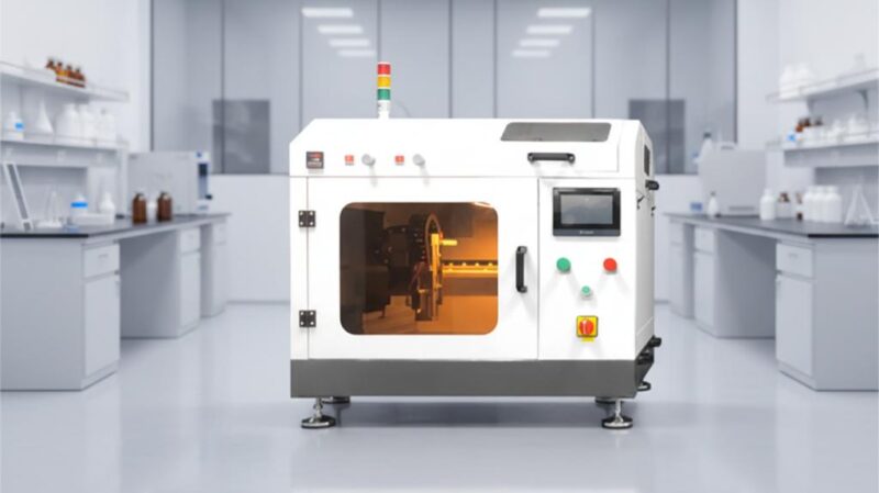
Ultrasonic Spray Deposition of Perovskite Functional Layers
Perovskite Solar Cells: Ideally suited for depositing perovskite light-absorbing layers, electron transport layers, and hole transport layers, where high uniformity is crucial for efficiency and stability.
Applications and Core Value of Ultrasonic Spray Coating Systems in Perovskite Functional Layer Deposition
Thanks to their high optical absorption coefficients, excellent charge-carrier mobility, and solution-processability, perovskite materials have emerged as prime candidates for next-generation photovoltaic and photodetection devices. The performance and stability of these devices depend heavily on the deposition quality of three key functional layers: the light-absorbing layer, the electron transport layer, and the hole transport layer. As a highly efficient solution-deposition technology, ultrasonic spray coating has become a pivotal tool for fabricating these layers; the high-uniformity thin films it produces are essential for ensuring efficient device operation and long-term stability.
Process Advantages of Ultrasonic Spray Coating: Overcoming Traditional Deposition Challenges
While traditional solution-deposition methods (such as spin coating) used for perovskite functional layers are simple to operate, they suffer from inherent limitations that are difficult to overcome. On one hand, centrifugal force causes a significant amount of precursor solution to be flung off during spin coating, resulting in material utilization rates typically below 30%—which drives up costs and causes environmental pollution. On the other hand, spin coating is prone to “edge effects” on large-area substrates, where the film thickness at the edges is noticeably thinner than in the center; uniformity deviations often exceed 15%, failing to meet the performance consistency requirements for large-scale device manufacturing.
Ultrasonic spray coating systems resolve these issues through a novel processing approach. The core principle involves using high-frequency ultrasonic vibrations (typically above 20 kHz) to atomize the functional layer precursor solution into tiny droplets with diameters of just 2–10 micrometers. Driven by a low-pressure gas stream, these droplets are sprayed uniformly onto a preheated substrate surface, where they rapidly dry and crystallize to form a thin film. Throughout the process, material utilization can exceed 80%. By precisely controlling the spray head’s movement trajectory, atomization pressure, and substrate temperature, edge effects are effectively avoided; even on large-area substrates, film thickness deviation can be kept within ±5%, laying the foundation for the uniformity of the functional layer.
Functional Layer Deposition: Ideal Applications for Ultrasonic Spraying Systems
Ultrasonic spraying systems are not merely “general-purpose equipment”; they enable targeted, high-quality deposition by optimizing process parameters to suit the specific characteristics of different functional layers. The uniformity of each type of functional layer is directly linked to the device’s core performance.
1. Perovskite Light-Absorbing Layer: Uniformity Determines Photogenerated Carrier Efficiency
The light-absorbing layer is the “core zone” where perovskite devices capture photons and generate photogenerated carriers; the uniformity of its film thickness and composition directly determines light absorption and carrier generation efficiencies. If the layer is locally too thick, carriers traveling to the electrode face increased recombination losses due to longer paths and a higher probability of collisions. Conversely, if it is locally too thin, photons may pass through the film without being fully absorbed. Both scenarios significantly reduce the device’s photoelectric conversion efficiency.
When depositing the light-absorbing layer, ultrasonic spraying systems achieve uniformity through a three-pronged parameter control strategy: first, adjusting atomization pressure to ensure consistent droplet size and prevent local accumulation caused by large droplets; second, setting a constant-speed movement path for the spray head to ensure uniform droplet coverage across the entire substrate; and third, matching the precursor solution concentration with the substrate temperature to control crystallization rates, thereby preventing compositional non-uniformity caused by excessively rapid local crystallization. Through this combined control approach, ultrasonic spraying systems produce light-absorbing layers with uniform thickness and high crystalline quality, ensuring uniform photon absorption across the substrate and maximizing carrier generation efficiency.
2. Electron Transport Layer: Uniformity Reduces Leakage Current Risk
The electron transport layer (ETL) is situated between the light-absorbing layer and the negative electrode. Its primary function is to rapidly extract electrons generated in the light-absorbing layer while blocking holes from migrating toward the negative electrode. The density and uniformity of the ETL film directly influence device leakage current and charge separation efficiency. ETLs fabricated via traditional methods (such as metal oxide layers) are prone to pinholes or localized thickness variations caused by droplet agglomeration. These defects act as “charge recombination channels”—where holes and electrons recombine prematurely before reaching the electrodes—generating significant leakage current and reducing the device’s fill factor (a key metric for charge collection efficiency).
When depositing the ETL, ultrasonic spraying systems use high-frequency atomization to break down the metal oxide solution into ultrafine droplets. As these droplets spread across the substrate surface, they naturally fill microscopic gaps, forming a continuous, dense, and pinhole-free film. Simultaneously, real-time monitoring of film thickness across different substrate regions allows for the dynamic adjustment of spray head dwell time, ensuring consistent thickness throughout the entire area. This uniformity not only blocks charge recombination channels but also lowers electron transport impedance, enabling lossless electron transport to the negative electrode and significantly enhancing the device’s charge separation efficiency.
3. Hole Transport Layer: Uniformity Ensures Efficient Charge Extraction
The hole transport layer (HTL) complements the ETL; located between the light-absorbing layer and the positive electrode, it is responsible for extracting and transporting holes. Its uniformity is likewise a critical factor in overall device performance. Localized defects in the HTL—such as thin spots or cracks—impede the transport path, preventing holes from reaching the positive electrode and causing them to recombine with electrons, which results in carrier loss. Conversely, excessively thick regions increase hole transport impedance and reduce transport speed.
In the deposition of hole transport layers, ultrasonic spray coating systems achieve uniformity through optimized drying processes: after atomized droplets are sprayed onto the substrate, the substrate is precisely heated to a specific temperature to allow for slow solvent evaporation, thereby preventing uneven film shrinkage caused by rapid drying. Simultaneously, the spray head employs a “cross-hatch” path design, ensuring that every area is evenly covered by droplets multiple times, resulting in a transport layer with consistent thickness and excellent interfacial contact. This uniformity not only reduces hole transport losses but also optimizes the interface between the light-absorbing layer and the anode, further enhancing the device’s overall photoelectric conversion efficiency.
The Core Value of High Uniformity: A Dual Guarantee of Efficiency and Stability
For perovskite devices, the high uniformity achieved by ultrasonic spray coating is not merely a “process detail” but a “core factor” determining the device’s performance ceiling and operational lifespan; its value is realized across the dimensions of both efficiency and stability.
Regarding efficiency, uniform functional layers minimize charge carrier losses. Uniformity in the light-absorbing layer ensures sufficient photon absorption, avoiding issues such as “insufficient absorption” or “excessive recombination”; meanwhile, uniformity in the electron and hole transport layers facilitates efficient charge transport channels, preventing charge recombination caused by defects. The synergistic effect of these layers can boost the device’s photoelectric conversion efficiency to over 90% of the best laboratory-scale levels. Furthermore, for large-area devices, this approach effectively avoids the common pitfall where “small-area devices are efficient while large-area ones fail,” thereby ensuring performance consistency in mass production.
Regarding stability, uniformity serves as the “first line of defense” against external degradation. During long-term operation, non-uniform films can develop localized stress due to differences in thermal expansion coefficients—varying degrees of thermal contraction between thick and thin regions make the film prone to cracking or delamination from the substrate, creating pathways for moisture and oxygen infiltration. Once external moisture and oxygen penetrate the device, they react chemically with the perovskite material, causing compositional degradation; consequently, device performance can plummet by more than 50% within just a few months. Highly uniform thin films produced by ultrasonic spraying equipment feature superior structural stability and uniform stress distribution; they effectively block the ingress of moisture and oxygen, extending device lifespans from months to years and clearing a critical hurdle for the industrialization of perovskite devices.
Technological Evolution: From “Uniformity” to “Precision”
As perovskite technology advances toward higher efficiency and longer lifespans, the process precision of ultrasonic spraying equipment is also continuously improving. Future developments will integrate AI-driven parameter optimization algorithms to enable “real-time monitoring and automatic adjustment” via closed-loop control, further limiting film thickness deviation to within ±2%. Simultaneously, the development of novel atomization units will allow for the precise control of droplet size, accommodating more complex functional layer compositions (such as mixed-cation perovskites). Furthermore, ultrasonic spraying equipment will be combined with processes like vacuum evaporation and laser annealing to create a “multi-process synergistic” manufacturing system, further enhancing functional layer quality and overall device performance.
In summary, the application of ultrasonic spraying equipment for depositing perovskite functional layers not only resolves the pain points associated with traditional processes but also ensures both high efficiency and stability through superior film uniformity. As perovskite technology moves toward industrialization, ultrasonic spraying equipment will serve as a core technology, driving the transition of next-generation optoelectronic devices from the laboratory to practical application.
About Cheersonic
Cheersonic is the leading developer and manufacturer of ultrasonic coating systems for applying precise, thin film coatings to protect, strengthen or smooth surfaces on parts and components for the microelectronics/electronics, alternative energy, medical and industrial markets, including specialized glass applications in construction and automotive.
Our coating solutions are environmentally-friendly, efficient and highly reliable, and enable dramatic reductions in overspray, savings in raw material, water and energy usage and provide improved process repeatability, transfer efficiency, high uniformity and reduced emissions.
Chinese Website: Cheersonic Provides Professional Coating Solutions
