
Ultrasonic Coating Machine for Photoresist Coating
Ultrasonic Coating Machine for Photoresist Coating – Cheersonic
In the process of semiconductor chip manufacturing breakthroughs towards 7nm and below advanced processes, photolithography, as a core and critical step in pattern transfer, directly determines the chip’s resolution and production yield. Exposure, as one of the most important steps in photolithography, directly depends on the coating quality of the photoresist (scientifically known as photoresist). Photolithography is the core process in semiconductor manufacturing that transfers mask patterns to semiconductor wafers. This process involves steps such as coating, pre-baking, exposure, development, and etching to replicate the pattern. Exposure is the core step where the photoresist undergoes a photosensitive reaction, forming a latent image, and is crucial in determining pattern accuracy. Chifei’s ultrasonic coating machine, with its core advantages of high precision, low damage, and high adaptability, perfectly meets the needs of photoresist coating. Its uniform and dense coating can accurately match various exposure processes and exposure dosage requirements, overcoming the pain point of poor compatibility between traditional coating and exposure. This provides core equipment support for improving the quality and efficiency of semiconductor photolithography processes and upgrading chip manufacturing processes, contributing to the breakthrough of domestic production in my country’s photolithography sector.
Exposure is the photosensitive process in photoresist where the photosensitive material absorbs light energy or other radiation energy. Technological iterations have continuously improved the precision of photolithography. Early exposure specifically referred to optical exposure. With the development of photolithography technology, the wavelength of the exposure light source has become shorter and shorter, even employing high-energy irradiation such as electron beams and ion beams to denature the photoresist and achieve nanoscale patterning. Although these high-energy particle sources or radiation sources are not light sources in the traditional sense, as an extension of optical photolithography technology, the industry still uses technical terms such as “light source,” “exposure,” “exposure amount,” and “lithography.” The core purpose of exposure is to allow the photoresist to absorb energy and undergo a photochemical reaction, laying the foundation for subsequent development and etching processes. The quality of exposure depends not only on the exposure equipment and parameter control but also on the uniformity and density of the photoresist coating—only a uniform and defect-free coating can ensure that the photosensitive material absorbs energy evenly, avoiding localized underexposure or overexposure, and guaranteeing the clarity and pattern precision of the latent image.
Contact exposure is one of the most widely used exposure methods currently, and its process flow and parameter control place stringent requirements on the quality of the photoresist coating. The core process of contact lithography is as follows: The exposure light source uses a mercury lamp or LED. After emitting ultraviolet light, it is shaped through optical path adjustment to form a nearly parallel beam covering a certain area. This beam illuminates a photomask, and the ultraviolet light passes through the transparent portion of the photomask, illuminating the photoresist film. This causes a photosensitive reaction in the photoresist, forming a latent image corresponding to the photomask. The most critical parameter in exposure is the exposure dose, calculated as: Exposure Dose = Exposure Intensity × Time. The precision of parameter control directly affects the lithography effect, and the calculation methods for different light sources vary significantly.
Mercury lamps and LEDs are the two most commonly used light sources in contact lithography. Their characteristics and parameter calculations must be strictly distinguished to avoid affecting the exposure results. When using mercury lamp light sources for photolithography, only the g, h, and i lines are typically used; other wavelengths are filtered out. Therefore, when calculating the exposure intensity, the measured intensity of a single wavelength needs to be multiplied by 2.5 to 3. LED light sources, on the other hand, are monochromatic, with the 365nm i-line being the most common. Their strong monochromaticity greatly benefits the morphology and process control of photoresist, effectively improving exposure consistency. When calculating exposure time, it is crucial to fully understand the equipment’s properties to avoid calculation errors. For example, if the photoresist requires an exposure dose of 100 mJ/cm², and the measured intensity of a mercury lamp at 365nm is 10 mW/cm², the required exposure time is (100 mJ/cm² ÷ 10 mW/cm²) ÷ 2.5 = 4 seconds. Furthermore, contact exposure has different exposure methods to adapt to different applications and meet the photolithography requirements of varying precision and batch sizes. Regardless of the exposure method, the photoresist coating must possess excellent uniformity and adaptability.
In the current field of photoresist coating, traditional coating processes (spin coating, high-pressure gas atomization spraying) have many shortcomings, which not only affect coating quality but also lead to poor compatibility with exposure processes, restricting photolithography accuracy and yield. Spin coating has a material utilization rate of less than 30%, wasting a large amount of expensive photoresist. Furthermore, high-speed rotation easily generates stress, resulting in uneven coating thickness. During exposure, the photosensitive material absorbs energy unevenly, leading to localized underexposure or overexposure, affecting latent image clarity. High-pressure gas atomization spraying easily introduces micro-dust impurities, and the high-pressure gas flow damages the photoresist’s activity. Uneven droplet size also results in pinholes and bubbles in the coating. After exposure, these defects are magnified, leading to blurred edges and reduced resolution. In addition, traditional spraying coatings have insufficient adhesion, easily peeling off after exposure, failing to meet the stringent accuracy requirements of advanced processes and increasing the trial-and-error costs of process optimization for companies.
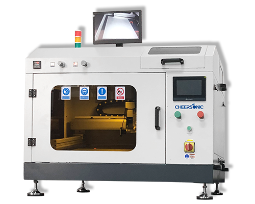
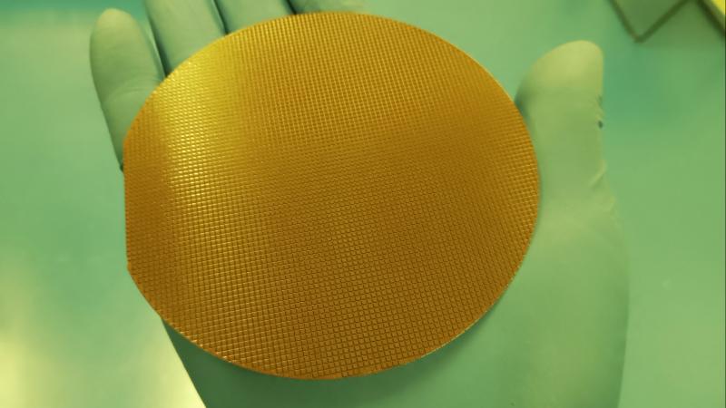
Chifei’s ultrasonic spray coating machine addresses the characteristics of photoresist, exposure process requirements, and pain points of traditional spray coating. Leveraging its core high-frequency ultrasonic atomization technology, it offers customized photoresist spraying solutions, achieving perfect compatibility between spraying and exposure processes. The equipment converts industrial frequency electricity into a 40-150kHz high-frequency electrical signal via an ultrasonic generator. This signal is then converted into high-frequency mechanical vibration by a piezoelectric ceramic transducer. Utilizing the ultrasonic cavitation effect, the photoresist is atomized into fine droplets of 0.01-2 microns, effectively de-agglomerating slurry particle clusters. This allows for precise control of coating thickness and uniformity, ensuring a dense, smooth coating free of pinholes and bubbles. It ensures uniform distribution of photosensitive materials, perfectly adapting to various exposure methods such as contact exposure, guaranteeing uniform energy absorption during exposure and meeting exposure dosage control requirements. The atomization process is conducted under low pressure and controlled temperature throughout, preventing damage to the photoresist’s activity while enhancing the adhesion between the coating and the wafer surface. This ensures the coating does not peel off or deform after exposure. Spraying parameters can be flexibly adjusted to adapt to the exposure needs of different light sources such as mercury lamps and LED i-lines, seamlessly integrating into integrated photolithography-exposure production lines.
Addressing the needs of photoresist spraying and exposure adaptation, Chifei ultrasonic spraying machines demonstrate four core advantages, helping semiconductor companies improve quality and reduce costs. First, ultra-precise and uniform coating, with a coating uniformity exceeding 99% and a thickness deviation ≤±1%, ensures uniform energy absorption during exposure, avoids localized exposure deviations, and guarantees latent image clarity and pattern accuracy. Second, strong exposure adaptability, with a dense coating and uniform distribution of photosensitive materials, adaptable to various methods such as contact exposure and electron beam exposure, compatible with mercury lamps and LED i-line light sources, and accurately matches exposure dosage calculation requirements. Third, high material utilization, reaching over 95%, significantly reduces photoresist waste, lowers production costs, and alleviates the pressure of relying on imports for high-end photoresists. Fourth, excellent mass production adaptability, supporting automated continuous spraying and adaptation to Class 100 cleanrooms, seamlessly integrating into automated photolithography-exposure production lines, adapting to different wafer sizes and photoresist types, and solving the problems of low efficiency, high waste, and poor exposure adaptability of traditional processes.
Currently, Chifei ultrasonic coating machines are widely used in photoresist coating scenarios, perfectly adapting to various exposure processes such as contact exposure. They cover positive and negative photoresists, as well as high-end photoresists like ArF and KrF, and are compatible with advanced lithography processes at 7nm and below. This helps domestic semiconductor companies solve problems such as poor compatibility between traditional coating and exposure, and low yield rates. As a leading company in the field of ultrasonic electronic equipment, Chifei Ultrasonic has been deeply involved in photoresist coating for many years, closely following the trend of exposure technology towards high precision and nanometer-level precision. Combined with the iterative needs of photoresist technology, it can provide customized solutions, covering the entire process from equipment selection and process parameter optimization to paste adaptation. In the future, Chifei Ultrasonic will continue to optimize equipment performance, further improve coating accuracy and exposure compatibility, help my country’s semiconductor lithography process break through technical bottlenecks, promote the localization and upgrading of the lithography process, and inject strong momentum into the high-quality development of the semiconductor industry.
About Cheersonic
Cheersonic is the leading developer and manufacturer of ultrasonic coating systems for applying precise, thin film coatings to protect, strengthen or smooth surfaces on parts and components for the microelectronics/electronics, alternative energy, medical and industrial markets, including specialized glass applications in construction and automotive.
Our coating solutions are environmentally-friendly, efficient and highly reliable, and enable dramatic reductions in overspray, savings in raw material, water and energy usage and provide improved process repeatability, transfer efficiency, high uniformity and reduced emissions.
Chinese Website: Cheersonic Provides Professional Coating Solutions
