
Photoresist Series: SU-8 Photoresist Performance, Processing, and Application Analysis
In the fields of micro/nano manufacturing and microstructure exploration, photoresist is a core functional material for achieving precise pattern transfer and constructing micro-devices, accurately outlining the detailed blueprints of the microscopic world. Among them, SU-8 photoresist, as a core category of epoxy resin-based negative photoresists, has become a key material in the manufacturing of microelectromechanical systems (MEMS), microfluidics, and precision optical devices due to its unique performance advantages. The industry continues to delve into the performance mechanisms and process adaptability of SU-8 photoresist, constantly optimizing coating and photolithography processing solutions to provide reliable technical support for micro/nano fabrication research and industrial production.
I. What is SU-8 Photoresist?
SU-8 photoresist is a classic epoxy resin-based negative photoresist. Its name originates from the eight epoxy groups contained in its molecular structure. These groups are the core foundation for achieving cross-linking curing and the formation of stable microstructures. So-called “negative photoresist” is characterized by a molecular cross-linking reaction in the UV-exposed areas, forming a stable, cured structure. The unexposed areas are completely washed away during the development process, ultimately pre-retaining the predetermined pattern structure, thus meeting the needs of various high-precision microstructure fabrication.
II. Core Material Characteristics of SU-8 Photoresist
SU-8 photoresist boasts excellent comprehensive performance, combining high precision, high stability, and high adaptability, making it a preferred material for thick-film micro/nano fabrication. Its core characteristics cover four dimensions: molding accuracy, physical properties, chemical properties, and optical properties.
In terms of molding and size adaptation, this photoresist exhibits excellent resolution, precision, and substrate adhesion, enabling the fabrication of complex, finely contoured micro-components. Under conventional processes, it can achieve spin-coating thicknesses from below 1μm to above 300μm, and can also fabricate thick-film structures exceeding 1mm in thickness through dry film lamination, demonstrating an extremely wide thickness adaptability range. Meanwhile, its imaging capabilities are outstanding, enabling the fabrication of microstructures with high aspect ratios. Under ultraviolet light exposure, the aspect ratio can reach 10:1, and under X-ray light exposure, it can reach 100:1. The verticality and regularity of the formed pattern are excellent, and high-quality patterns with vertical sidewalls can be achieved even in millimeter-thick films.
In terms of optical performance, SU-8 photoresist exhibits extremely low light absorption in the 365nm-400nm near-ultraviolet wavelength range, allowing light to penetrate the entire photoresist layer uniformly. This ensures consistent exposure across the entire photoresist layer, effectively avoiding problems such as uneven local exposure and pattern distortion. The final thick-film pattern possesses excellent characteristics such as vertical sidewalls and a high aspect ratio.
In terms of mechanical and chemical stability, SU-8 photoresist exhibits high mechanical strength after curing, withstanding chemical mechanical polishing processes to meet the requirements of device planarization. It can also stably fabricate complex microstructures containing steps and irregular shapes. Its thermal and chemical stability is excellent, with resistance to corrosion and high temperatures, and it possesses good biocompatibility, making it suitable for special applications such as life sciences and biosensing. Furthermore, the cured SU-8 photoresist layer exhibits excellent insulation properties and can be directly used as an insulating structure in electroplating processes.
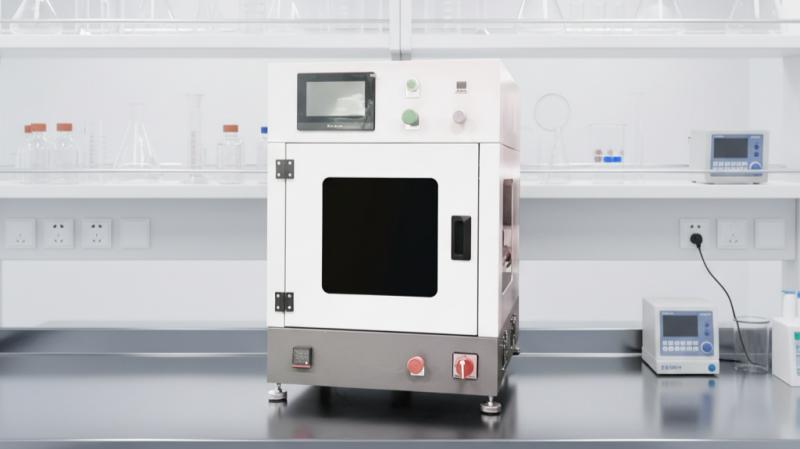
III. Ultrasonic Spraying: A Novel Coating Process for SU-8 Photoresist
Traditional SU-8 photoresist processing primarily utilizes spin coating, currently the most widely used method, but it has significant limitations. Spray coating relies on centrifugal force to spread the photoresist layer, which easily leads to edge buildup and uneven overall thickness. When dealing with deep trenches, micropores, and irregularly shaped 3D microstructures, it is prone to defects such as coating gaps and missed areas. Simultaneously, in traditional contact mask lithography, the mask must be in close contact with the photoresist layer. Over long-term processing, photoresist adhesion to the mask can occur, not only reducing lithographic resolution but also causing irreversible damage to the chromium structure of the mask, increasing production costs and defect rates.
To overcome the limitations of traditional processes, ultrasonic spraying technology is gradually being applied to the SU-8 photoresist coating process, becoming a core process solution for high-precision, complex microstructure processing. This technology utilizes high-frequency ultrasonic vibration to atomize liquid SU-8 photoresist into micron-sized, uniform droplets. Precise airflow then guides these droplets to gently and uniformly deposit on the substrate surface, achieving contactless precision coating.
Compared to traditional spin coating, ultrasonic spraying offers greater adaptability, completely resolving the uneven coating and edge buildup issues caused by centrifugal force in spin coating. It can penetrate deep into complex three-dimensional structures such as high aspect ratio trenches and micropores, achieving complete coverage without dead angles and effectively eliminating process defects such as voids and uneven thickness. Simultaneously, the contactless spraying mode avoids surface scratches and photoresist contamination, maximizing the protection of the delicate microstructure substrate. In terms of thickness control, ultrasonic spraying allows for precise parameter adjustment of the photoresist layer thickness, resulting in extremely high process stability and repeatability, significantly improving device performance consistency. Furthermore, this process has a much higher material utilization rate than traditional processes, significantly reducing photoresist waste, lowering processing costs, and making it suitable for large-scale production and high-precision scientific research experiments.
IV. Core Application Areas of SU-8 Photoresist
Thanks to its excellent comprehensive performance and the empowerment of the new ultrasonic spraying process, the application scenarios of SU-8 photoresist continue to expand. It has now become a core material in fields such as MEMS (Micro-Electro-Mechanical Systems), microfluidic chips, precision optical devices, sensing and detection, and special electroplating.
In the field of precision optics, it can be used to fabricate core optical devices such as optical waveguides and microlens arrays. It offers high forming precision and good optical transmittance, meeting the requirements of precision optical systems. In the field of MEMS (Micro-Mechanical Systems), it can be used to mass-produce micro-motor arrays, micro-mechanical components, and electroplating molds. Its high mechanical strength and structural stability ensure the operational accuracy and lifespan of micro-devices.
In the field of microfluidic chips, the application of SU-8 photoresist is particularly extensive. It can precisely fabricate core functional structures such as microchannels, reaction chambers, micro-valves, and micro-pumps. It can also be used as an encapsulation material to process chip top and bottom covers, connectors, and sealing structures, achieving overall encapsulation of microfluidic chips. Combined with the uniform coating advantage of ultrasonic spraying, it can significantly improve the forming quality of complex flow channel structures and chip yield.
In addition, SU-8 photoresist is widely used in the fabrication of various micro-sensors and micro/nano functional structures. Leveraging its excellent biocompatibility, it is suitable for life science-related scenarios such as biological detection and microscopic biochemical experiments, demonstrating extremely high application value.
V. Summary and Development Prospects
In the current era of rapid development in micro/nano manufacturing technology, SU-8 photoresist, with its unique advantages such as high resolution, high aspect ratio molding capability, and excellent mechanical, chemical, and biocompatibility, has become an indispensable core material in the fields of MEMS, microfluidics, and precision micromachining. Its adaptability to thick films, irregular shapes, and high-precision microstructure molding compensates for the shortcomings of ordinary photoresists in thick-layer processing and complex structure processing, providing core support for the precision and integration of micro-devices.
Meanwhile, the iterative upgrades of new coating processes such as ultrasonic spraying have further broken through the processing limitations of SU-8 photoresist, solving the pain points of insufficient precision, poor adaptability, and material waste in traditional processes. This allows SU-8 photoresist to better adapt to high-end processing scenarios such as three-dimensional complex microstructures, ultra-thick films, and precision flexible substrates. With the continuous development of micro-nano manufacturing, life sciences, precision sensing and other fields, the application boundaries of SU-8 photoresist will continue to expand, and the supporting processing technology will also be continuously optimized. In the future, it will play a more important role in the research and development of high-end micro-nano devices and precision intelligent manufacturing, and continuously promote the technological upgrading of the micro-processing industry.
About Cheersonic
Cheersonic is the leading developer and manufacturer of ultrasonic coating systems for applying precise, thin film coatings to protect, strengthen or smooth surfaces on parts and components for the microelectronics/electronics, alternative energy, medical and industrial markets, including specialized glass applications in construction and automotive.
Our coating solutions are environmentally-friendly, efficient and highly reliable, and enable dramatic reductions in overspray, savings in raw material, water and energy usage and provide improved process repeatability, transfer efficiency, high uniformity and reduced emissions.
Chinese Website: Cheersonic Provides Professional Coating Solutions
