
A Comprehensive Analysis of the Photoresist Industry Chain
I. Photoresist Industry Chain Overview
– Upstream: Photoresist raw materials such as resins, monomers, photoinitiators, and solvents
– Midstream: Photoresist formulation R&D, production synthesis, and quality control
– Downstream: Printed circuit boards, flat panel displays, semiconductor chips, microelectromechanical systems, etc., applied in consumer electronics, home appliances, automotive electronics, and other fields
Photoresist is the material with the highest technological barriers in the fine chemical industry and is a core material for semiconductor manufacturing. Industry development is driven by downstream demand, with downstream process upgrades forcing material technology iteration, and domestic substitution and capacity expansion bringing incremental market growth. High barriers exist at each stage of the industry chain, with stable upstream certification and procurement models and close cooperative relationships.
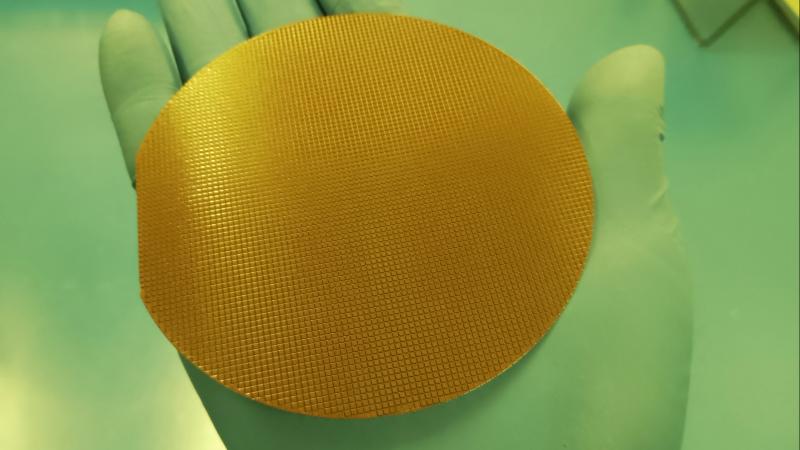
II. Photoresist Industry Overview
Core Definition: Photoresist is a key pattern transfer medium in the photolithography process. It achieves pattern transfer through exposure, development, and etching, directly affecting product accuracy and yield. Its main components are resin, photoinitiator, solvent, and additives, with resin being the primary component.
Market Size
– Global market size continues to grow, with high-end products dominating the market.
– Domestic market size is steadily increasing, with production capacity concentrated on low- and mid-range products.
Driven Factors
1. Policy: Promotion of domestic substitution, focusing on breakthroughs in high-end technologies.
2. Technology: AI development drives process upgrades, increasing the precision requirements for photoresist.
3. Industry: Wafer fab expansion, memory technology upgrades, and stable, inelastic demand.
Industry Barriers
Long certification cycles, high technical formulation barriers, reliance on external suppliers for upstream raw materials, and limited production equipment—these four barriers constrain industry development.
III. Upstream of the Industry Chain (Raw Materials)
1. Resins and Monomers
– Resins are the main component for film formation, accounting for nearly 50% of the cost, requiring high chemical stability and photosensitivity.
– High-purity monomers are the core of resin synthesis, with extremely high requirements for purity and batch stability.
– High-end resin molecular design and polymerization processes are highly complex, representing a core barrier to domestic substitution.
2. Photoinitiators
– Initiate chemical reactions under light, altering resin solubility to complete photolithography.
– Usage accounts for 3%-5%, cost accounts for 10%-15%.
– High technological barriers, high market concentration, and a clear trend of the industry chain shifting to China.
3. Solvents
– Largest component, used to dissolve raw materials, adjust viscosity, and assist in coating and cleaning.
– High-end applications have stringent requirements for solvent purity; China has achieved breakthroughs in some high-end solvent technologies.
IV. Midstream of the Industry Chain (Manufacturing)
Product Classification
1. By Development Characteristics: Positive Photoresist, Negative Photoresist
2. By Application Area: Panel Photoresist, PCB Photoresist, Semiconductor Photoresist
Product Sub-categories
– Panel Photoresist: Used in display panel manufacturing, including TFT, color, black and white, and touchscreen photoresists.
– PCB Photoresist: Used for circuit pattern transfer on circuit boards, including dry film, wet film, and photo-imaging solder resist inks. Domestic substitution rate is relatively high.
– Semiconductor Photoresist: Highest technological barrier, categorized by exposure light source as G-line, I-line, KrF, ArF, EUV, etc.; shorter wavelengths result in higher resolution. High-end products have long certification cycles and strong customer loyalty.
V. Downstream Industry Chain (Application Scenarios)
1. Semiconductor Manufacturing: Accounts for approximately 45% of total demand. Logic chips use high-end ArF and EUV photoresists, while memory chips primarily use KrF. Wafer capacity expansion brings significant demand.
2. Display Panels: Used in the production of LCD, OLED, and TFT panels. Mature technology, high domestic sourcing rate.
3. PCB and Advanced Packaging: PCB photoresist substitution rate exceeds 90%; advanced packaging requires thicker films and higher etching resistance, leading to rapid demand growth.
4. Procurement Characteristics: Long downstream customer certification cycles, stable cooperation, significant first-mover advantage.
5. Demand Trends: Growth in demand for high-end chips is driving peak demand for ArF and EUV photoresists.
VI. Industry Outlook
1. Deepening Industry Collaboration: Materials, wafer, and equipment manufacturers are deeply integrated and engaging in joint R&D.
2. Domestic Production Upgrade: Shifting from “mass production” to “stable supply, cost optimization, and technological iteration.”
3. Accelerated Industry Consolidation: Mergers and acquisitions are becoming an important way to acquire technology, talent, and market access.
Overall, the development of next-generation information technology will continue to drive the growth in demand for high-precision chips and photoresists, leading the industry towards high-end, collaborative, and integrated development.
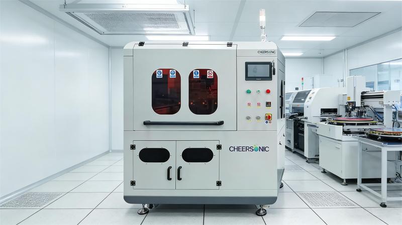
Currently, ultrasonic spraying of photoresist has gradually replaced some traditional coating processes, becoming the preferred solution for irregular structures, large-size substrates, flexible electronics, and high-precision micro-nano processing scenarios. It effectively solves the pain points of traditional photoresist coating processes and plays an important role in improving product processing accuracy, reducing production costs, and expanding the application scenarios of photolithography. It is one of the important development directions of advanced photolithography manufacturing processes.
About Cheersonic
Cheersonic is the leading developer and manufacturer of ultrasonic coating systems for applying precise, thin film coatings to protect, strengthen or smooth surfaces on parts and components for the microelectronics/electronics, alternative energy, medical and industrial markets, including specialized glass applications in construction and automotive.
Our coating solutions are environmentally-friendly, efficient and highly reliable, and enable dramatic reductions in overspray, savings in raw material, water and energy usage and provide improved process repeatability, transfer efficiency, high uniformity and reduced emissions.
Chinese Website: Cheersonic Provides Professional Coating Solutions
