
Advanced Packaging Technology Popular Science
The Post-Moore’s Law Era: Advanced Packaging Becomes a Core Technology Direction
1. Moore’s Law Slows Down
– Wafer manufacturing physical properties are approaching their limits. The shrinking of transistor sizes has led to problems such as quantum tunneling, extending the process update cycle from 18 months to 3 years.
– Advanced process R&D costs are rising sharply. The design costs of 5nm, 3nm, and 2nm chips continue to increase, and the performance improvement rate is gradually narrowing. High-end process capacity is concentrated in a few manufacturers, making it difficult for smaller customers to obtain it.
2. Three Major Development Directions of Integrated Circuits
– Deep Moore’s Law: Continuing the trend of shrinking CMOS, innovating in device structure and wiring to further improve chip performance.
– Beyond Moore’s Law: Achieving system-level integration of processing, analog/RF, optoelectronic, and sensing functions through advanced packaging to improve overall system performance.
– New Devices: Utilizing new devices other than CMOS to break through the performance limitations of traditional integrated circuits.
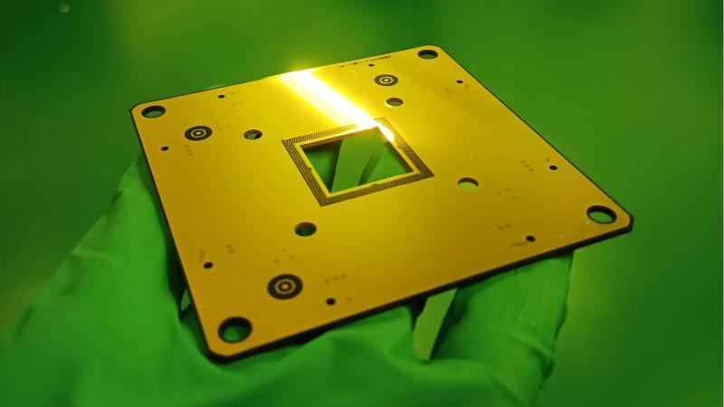
Core Processes of Advanced Packaging
Four Basic Elements
Advanced packaging can be defined by possessing any one of the following: bump, redistribution layer (RDL), through-silicon via (TSV), or wafer.
– Bump: Enables interface interconnection and stress buffering. Future sizes and spacing will continue to shrink, gradually evolving towards bump-free bonding.
– Redistribution Layer (RDL): Enables electrical extension in the XY plane, an essential process for 2.5D/3D packaging.
– Through-silicon Via (TSV): Enables vertical electrical extension along the Z-axis, a key technology in the transition from 2D to 3D packaging, shortening interconnect paths, reducing power consumption, and improving communication speed.
– Wafer: As the carrier of integrated circuits, its size continues to increase, with TSV aspect ratios improving and via diameter and spacing shrinking.
Detailed Explanation of Key Processes
1. Bump
– Conductive bumps on the chip surface, replacing traditional leads to achieve electrical interconnection, heat transfer, and mechanical support.
– Widely used in mid-to-high-end packaging such as ball grid arrays, chip-scale, and flip chips, it is a core technology for area array packaging.
2. Through-Silicon Vias (TSV)
– Creates vertical vias between chips/wafers and fills them with metal to achieve vertical interconnection.
– Divided into post-via processes, it simplifies the process and is widely used in image sensors and MEMS devices.
3. Temporary Bonding/Debonding (TBDB)
– When wafers are thinned to below 100μm, they are prone to warping and cracking, requiring temporary carriers and adhesives for support, which are then separated after the process is complete.
– It is a core solution for back-end processing of large-size ultra-thin wafers, supporting TSV manufacturing and multi-wafer stacking.
4. Chiplets
– Enables heterogeneous integration, integrating chips with different functions and processes to improve the overall performance of integrated circuits.
Mainstream Packaging Technology Types
1. 2.5D Packaging: Achieves side-by-side integration of multiple chips using an adapter board, balancing cost and performance.
2. 3D Packaging: Vertically stacking chips/wafers significantly saves space, increases interconnect density, reduces parasitic effects, and optimizes yield and cost.
Core Materials for Advanced Packaging (Clear Incremental Demand)
Iterative advancements in advanced packaging processes drive demand growth for various materials. 2.5D/3D packaging adds etching, deposition, and polishing processes, further expanding the materials market.
1. IC Carrier (Packaging Substrate)
– The bridge between the chip and external circuitry, providing mechanical support, heat dissipation, and electrical interconnection.
– Flip-chip substrates are the mainstream for advanced packaging, accounting for a high cost proportion. Demand for high-end carriers continues to grow with upgrades in computing power and packaging technology, while the supply of upstream core raw materials constrains capacity expansion.
2. Electroplating Solution
– Used for bump and redistribution layer manufacturing and through-silicon via (TSV) metal filling; a core consumable in the electroplating process.
– Copper interconnects represent the largest sub-market. Copper electroplating is suitable for filling large-size TSVs, offering advantages such as high speed, good uniformity, and high process compatibility.
3. Epoxy Molding Compound (EMC)
– Holds a dominant market share in encapsulation materials, used for chip protection, providing thermal conductivity, insulation, moisture resistance, and pressure resistance.
– Advanced packaging demands higher reliability and electrical performance, requiring customized formulations based on process and customer needs.
4. Electronic Adhesives
– Used for component protection, electrical connections, structural bonding, thermal management, and electromagnetic shielding.
– Subcategories include chip bonding materials and underfill adhesives. Underfill adhesives are key materials for flip-chip and 2.5D/3D packaging, mitigating thermal expansion stress and improving chip reliability.
– Spherical silicon micropowder is a core inorganic filler in IC substrates, epoxy molding compounds, and underfill adhesives; high-end applications primarily utilize spherical silicon micropowder.
5. Photolithography Materials
– Includes photoresist, PSPI, and photomasks, and is a core consumable for high-precision circuit pattern transfer.
– Used in high-density substrates, bump forming, redistribution layers, through-silicon vias (TSVs), and wafer-level packaging, meeting the needs of high-precision line manufacturing.
6. CMP Materials
– Includes polishing slurries, polishing pads, etc., achieving high surface planarization of the wafer through chemical and mechanical processes.
– Through-Silicon Vias (TSV) polishing is divided into front-side barrier layer polishing and back-side wafer polishing, adapting to different TSV process requirements.
7. Temporary Bonding Adhesive
– The bonding interlayer between the wafer and the temporary substrate, a key material for wafer thinning.
– Requires excellent thermal stability, bond strength, and mechanical stability. It is divided into three categories: wax-like substances, composite tapes, and spin-coating adhesives, with spin-coating adhesives being the most widely used.
Market and Development Trends
1. Market Size: Driven by AI and high-performance computing, the global advanced packaging market share continues to increase, with a considerable compound annual growth rate; the domestic advanced packaging output value is lower than the global average, indicating broad potential for domestic production.
2. Equipment Investment: Global semiconductor equipment investment has rebounded rapidly after a short-term adjustment, supporting the expansion of the advanced packaging industry.
3. Industry Trends: Advanced packaging is developing towards high density, miniaturization, 3D stacking, and heterogeneous integration; domestic materials and processes, leveraging market space, cost, and supporting advantages, are poised for domestic substitution opportunities.
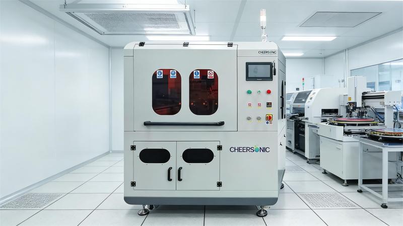
New Process Equipment: Application of Ultrasonic Spray Coating Machines in Advanced Semiconductor Packaging
Ultrasonic spray coating machines utilize high-frequency ultrasonic atomization technology to uniformly, ultra-thinly, and non-damagingly coat functional materials for packaging, such as photoresist, underfill, temporary bonding adhesive, insulating coating, and conductive film, onto the surfaces of wafers, chips, and packaging substrates. In advanced semiconductor packaging, its core application value lies in:
Excellent Coating Uniformity: Achieves ultra-thin, uniform film formation at the nanometer to micrometer level, meeting the requirements of high-precision processes such as RDL, TSV, and bump fabrication for thin, uniform coatings.
High Material Utilization: Fine and controllable atomized particles significantly reduce material waste and are compatible with high-cost packaging-specific chemicals.
No high-pressure impact: The spraying process is gentle, avoiding stress, warping, or damage to ultra-thin wafers, fragile chips, and microstructures. It is suitable for delicate processes such as 3D stacking and chiplet heterogeneous integration.
Strong process compatibility: It can adapt to various materials such as photoresists, electronic adhesives, insulating media, and thermally conductive coatings, and is compatible with 8-inch and 12-inch large-size wafers and advanced packaging processes, improving packaging yield and reliability.
As advanced packaging develops towards thinner, denser, and higher integration, ultrasonic spraying has become a new key process equipment in photolithography, coating, and thin film preparation.
About Cheersonic
Cheersonic is the leading developer and manufacturer of ultrasonic coating systems for applying precise, thin film coatings to protect, strengthen or smooth surfaces on parts and components for the microelectronics/electronics, alternative energy, medical and industrial markets, including specialized glass applications in construction and automotive.
Our coating solutions are environmentally-friendly, efficient and highly reliable, and enable dramatic reductions in overspray, savings in raw material, water and energy usage and provide improved process repeatability, transfer efficiency, high uniformity and reduced emissions.
Chinese Website: Cheersonic Provides Professional Coating Solutions
