
Advanced Packaging Photoresist and Its Development Trends
Applications of Photoresist in Advanced Packaging
Photoresist, also known as photoresist material, is a core consumable in microfabrication. Its solubility changes after exposure to a light source, making it an etch-resistant material. It is an auxiliary material in advanced packaging manufacturing, primarily used for creating metal patterns in redistribution layers. After the process is complete, it is stripped away and does not remain on the device.
With the increasing demand for miniaturization and high integration in integrated circuits, photolithography technology and photoresist are widely used in advanced packaging scenarios such as high-density substrates and interposer layers, redistribution layers, TSVs, high-density flip-chip bump forming, and wafer-level packaging.
Currently, advanced packaging often employs thick-film photolithography technology with micron-level resolution and thicknesses ranging from several microns to tens of microns, combined with electroplating processes to fabricate copper bumps with pitches of tens of microns.
Basic Photolithography Process
1. Coating the substrate surface with a photoresist film
2. Exposure of the photoresist through a photomask; a photochemical reaction occurs (positive photoresist decomposes in light, negative photoresist cures in light)
3. Development to remove photoresist from exposed/unexposed areas
4. During the etching process, the photoresist protects the corresponding areas, completing pattern transfer.
As line sizes shrink, the requirements for high resolution, high aspect ratio, rapid development, and complete stripping continue to increase. General-purpose photoresists for integrated circuits can meet the basic resolution and thickness requirements of advanced packaging.
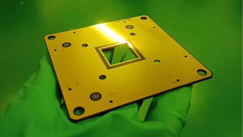
Photoresist Categories and Material Characteristics
Core Technical Parameters
1. Resolution: The minimum linewidth achievable by the process, affected by photoresist characteristics and the wavelength of the exposure light source; positive photoresists have better resolution than negative photoresists.
2. Contrast Ratio: The ability to distinguish between exposed and unexposed areas; higher contrast ratios result in clearer pattern edges.
3. Sensitivity: The degree to which the photoresist reacts to light, determining exposure speed and production efficiency. 4. Corrosion Resistance: Includes heat resistance, chemical corrosion resistance, plasma bombardment resistance, and ion implantation resistance, ensuring the stability of subsequent processes.
5. Viscosity: Affects film thickness; advanced packaging requires thicker adhesives with higher viscosity.
6. Adhesion: Bonding strength to the substrate, preventing peeling during processing and ensuring film uniformity.
Main Classifications
By Solubility Changes
– Positive Resins: Dissolve and decompose in the exposed area, resulting in a pattern consistent with the mask after development; high resolution, but weaker adhesion and etching resistance, and higher cost.
– Negative Resins: Cross-link and solidify in the exposed area, resulting in a pattern opposite to the mask after development; good adhesion, fast photosensitivity, prone to swelling during development, and lower resolution.
By Exposure Light Source
Advanced packaging mainly uses ultraviolet photoresists, including g-line (436nm) and i-line (365nm); in addition, there are deep ultraviolet (DUV), extreme ultraviolet (EUV), electron beam, X-ray, and ion beam photoresists.
1. UV Positive Photoresist
– Mainstream Systems: Phenolic resin-diazonaphthoquinone system, chemical amplification system
– Applicable Linewidths: Broadband 2~3μm/0.8~1.2μm; g-line 0.5~0.6μm; i-line 0.35~0.5μm
2. UV Negative Photoresist
– Mainstream Systems: Polyvinyl alcohol cinnamate system, cyclized rubber-diazid system
– Applicable Linewidths: Greater than 0.35μm
New Technology and Material Development
The current pattern resolution of advanced packaging is in the micrometer to ten-micrometer range, and will develop towards submicrometer and nanometer levels in the future. Photoresists will continue to upgrade with the iteration of exposure light sources.
1. Deep Ultraviolet (DUV) Photoresist
– Employs chemical amplification technology, with photo-induced acid-generating agent catalytic reaction, significantly improving sensitivity.
– 248nm Photoresist: Compatible with KrF light sources, used for the fabrication of 0.25~0.15μm devices. 1. **193nm Photoresist:** Compatible with ArF light sources, optimized for dry etching resistance and adhesion, already in large-scale application.
2. Extreme Ultraviolet (EUV) Photoresist: Wavelength 10-14nm, resolution up to 10nm, the next-generation mainstream photolithography technology.
Requirements: Low absorptivity, high transmittance, strong etching resistance, low exposure energy.
3. Electron Beam Photoresist:Resolution up to 5-30nm, used for mask and micro/nano device fabrication.
Negative photoresist: High sensitivity, prone to swelling during development; Positive photoresist: Higher resolution, lower sensitivity.
4. X-ray Photoresist:Primarily used in MEMS LIGA technology, suitable for high aspect ratio, thick 3D structures.
Advantages: High resolution, deep focus; Limitations: High light source cost.
5. Ion Beam Photoresist
– Can simultaneously complete exposure, etching, and deposition, simplifying the process; however, production efficiency is relatively low, limiting commercialization.
6. Nanoimprint Photoresist
– Not limited by light source wavelength, offering high resolution and low cost.
– Currently in the laboratory stage; mask preparation and process stability require further breakthroughs.
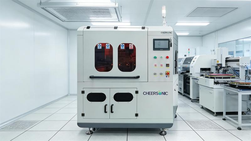
Ultrasonic spraying technology has become the preferred process for photoresist coating in advanced packaging. With its precise and controllable atomization spraying method, it can achieve ultra-thin, uniform, and bubble-free photoresist film deposition. Compared to traditional spin coating processes, this technology significantly improves material utilization, effectively saving on high-end photoresist consumable costs, and is compatible with various precision processes such as wafer-level packaging, fan-out, and 2.5D/3D packaging. The equipment’s spray flow rate and atomization particle size are adjustable, meeting the needs for preparing photoresist layers of different thicknesses. The coating edge contours are clear, and the thickness consistency is high, effectively improving the accuracy of subsequent photolithography exposure, development, and etching processes. Its low-temperature spraying characteristics will not damage the precision chip substrate, and the process stability is strong, which helps the advanced packaging industry achieve efficient mass production and promotes the steady upgrading of high-end semiconductor packaging technology towards refinement and low cost.
About Cheersonic
Cheersonic is the leading developer and manufacturer of ultrasonic coating systems for applying precise, thin film coatings to protect, strengthen or smooth surfaces on parts and components for the microelectronics/electronics, alternative energy, medical and industrial markets, including specialized glass applications in construction and automotive.
Our coating solutions are environmentally-friendly, efficient and highly reliable, and enable dramatic reductions in overspray, savings in raw material, water and energy usage and provide improved process repeatability, transfer efficiency, high uniformity and reduced emissions.
Chinese Website: Cheersonic Provides Professional Coating Solutions
