
Semiconductor Photoresist for Back-End Packaging
Photoresist is not only used in front-end chip manufacturing, but also has its own category in advanced packaging. It is a key material supporting chip miniaturization, high performance, and low power consumption. The core of advanced packaging is to shorten chip interface spacing and interconnect length, increase interface density, and achieve heterogeneous integration of multiple chips. Bumps and redistribution layers (RDLs) are two key technologies, and photoresist provides core support for them.
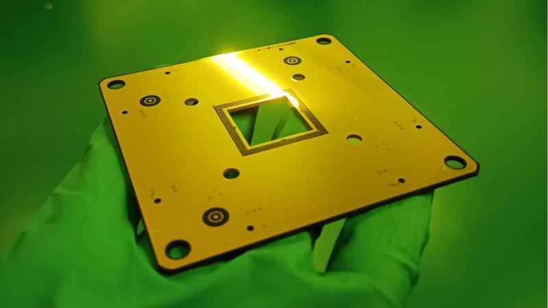
I. Bump Process and Photoresist
1. Function: As the “pins” for chip electrical connections, it undertakes the electrical connections between the chip and the substrate, and between chips, and is a core component of multi-chip integration.
2. Manufacturing Process: Wafer cleaning → Deposition of barrier and seed layers → Photoresist coating, exposure and development for patterning → Electroplating to form the UBM layer → Photoresist removal and etching → Ball placement and heat bonding.
3. Function of Photoresist: Patterning defines the position and shape of bumps, providing a template for electroplating; thick-film photoresist supports bump formation and, together with a passivation layer, provides insulation protection.
4. Materials and Parameters: Bump material contains gold, copper, tin, etc.; photoresist coating thickness ≤ 110 micrometers.
5. Material Requirements: Thick film characteristics, high aspect ratio, able to withstand high-temperature reflow soldering above 200℃, and resistant to electroplating solution corrosion.
II. Redistribution Layer (RDL) Process and Photoresist
1. Function: Rearranges chip I/O interfaces, fanning out dense pins to the substrate, enabling multi-chip interconnection and heterogeneous integration.
2. Fabrication Flow: Wafer cleaning → First photolithography layer → UBM layer deposition → Photoresist coating and pattern definition → Copper electroplating to form circuitry → Photoresist removal and etching → Second photolithography layer for reinforcement and protection.
3. Process Characteristics: Multilayer stacking process, mainstream layer count 6-8 layers, high-end applications reach 10 layers or more, each layer requires precise photoresist definition of the circuitry.
4. Material Requirements: High resolution, adaptable to <150℃ low-temperature processes, low defects, ensuring accurate overlay of multilayer circuitry.
III. Core Products and Application Scenarios of Advanced Packaging Photoresists
1. General-purpose photoresists: Suitable for traditional packaging, low-to-medium level bumps, and low-to-medium density RDL wiring, covering basic packaging needs.
2. High-end bump-specific photoresists: Suitable for high-end scenarios such as 3D TSV, HBM, and AI chips. Some products support ultra-thick coatings and high-temperature resistance, meeting the large bump requirements of power devices.
3. High-end RDL-specific photoresists: High technological barriers, suitable for multi-layer RDL processes, a core material for high-end packaging scenarios, and also has advantages in the field of ultra-thick bump photoresists.
4. Subcategories: 3D packaging/TSV-specific photoresists, a full range of high-end bump/RDL photoresists, with mature supporting resin technology.
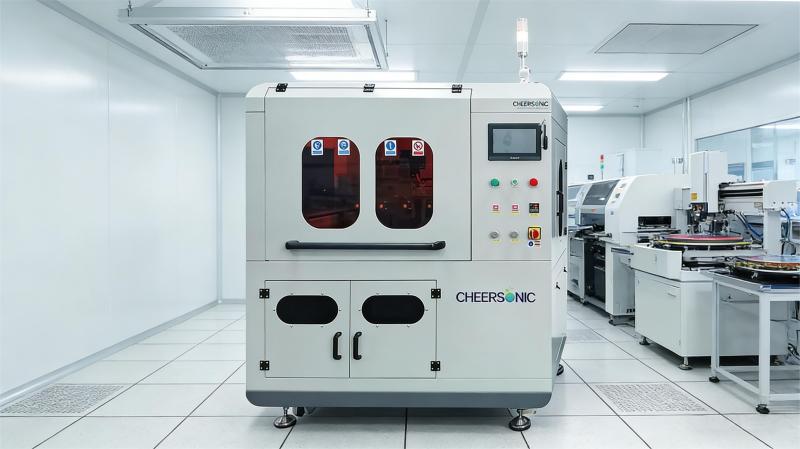
In the field of advanced semiconductor packaging, ultrasonic spray coating machines have become the core preferred equipment for precise photoresist coating. Based on the principle of high-frequency oscillation atomization, the equipment can uniformly refine photoresist into micron-sized droplets, eliminating the drawbacks of traditional spin coating such as wasteful thick layers and uneven edge thickness. It perfectly adapts to the requirements of high-end packaging processes such as fan-out and 2.5D/3D stacking. The spraying process features controllable flow rate and strong coating consistency, forming a thin, dense, and highly adhesive photoresist film layer on the surface of chip wafers and micro-components, significantly improving photolithography imaging accuracy and pattern transfer yield. Simultaneously, the equipment boasts low consumable consumption and broad process compatibility, adapting to various photoresist materials of different viscosities. This simplifies packaging production line processes, effectively reducing manufacturing costs and helping the advanced semiconductor packaging industry steadily upgrade towards high precision, high efficiency, and low cost.
About Cheersonic
Cheersonic is the leading developer and manufacturer of ultrasonic coating systems for applying precise, thin film coatings to protect, strengthen or smooth surfaces on parts and components for the microelectronics/electronics, alternative energy, medical and industrial markets, including specialized glass applications in construction and automotive.
Our coating solutions are environmentally-friendly, efficient and highly reliable, and enable dramatic reductions in overspray, savings in raw material, water and energy usage and provide improved process repeatability, transfer efficiency, high uniformity and reduced emissions.
Chinese Website: Cheersonic Provides Professional Coating Solutions
