
Megasonic Cleaning for Wafer Processing
Megasonic cleaning has become an indispensable key technology in multiple high-tech fields, especially in the wafer processing stage of semiconductor manufacturing. With the development of electronic devices towards smaller sizes and stronger performance, the demand for ultra clean wafer surfaces is increasing day by day. High frequency sound wave cleaning effectively removes pollutants by emitting high-frequency sound waves to excite the cleaning solution without damaging the fragile surface of the wafer, providing an advanced and reliable solution for achieving high cleanliness.
This technology is based on high-frequency sound waves at the megahertz level acting on cleaning liquids to excite the formation of micrometer sized bubbles. These bubbles continue to oscillate and implode under the influence of the sound field, producing the “cavitation effect”. Compared with traditional ultrasonic cleaning using low-frequency sound waves, high-frequency sound wave cleaning generates smaller bubble sizes and milder cavitation effects, making it particularly suitable for cleaning semiconductor wafers with fine structures and complex patterns.

High frequency sound waves can achieve a more uniform energy distribution throughout the entire cleaning solution, thereby improving the accuracy and controllability of the cleaning process. Micro cavitation bubbles can effectively remove sub micron particles and pollutants, making them perform excellently in wafer cleaning with precise structures.
Main applications in wafer processing
- Removal of particulate pollutants
A key application of high-frequency acoustic cleaning in wafer processing is the removal of particulate contaminants. With the increasing complexity of semiconductor device structures, even tiny particle residues may cause defects and reduce yield. This technology can efficiently remove particles attached to the wafer surface, ensuring high cleanliness standards and reducing the risk of defects in subsequent processes. - Thin film and oxide layer removal
In the photolithography, etching and other processes of wafer processing, unnecessary thin films or oxide layers are often formed. High frequency acoustic cleaning can selectively remove such surface substances without damaging the underlying structure, balancing cleaning effectiveness and process safety. - Strengthen the chemical cleaning effect
This technology is often used in conjunction with chemical cleaning methods to enhance overall cleaning efficiency. High frequency sound waves help to evenly distribute chemical reagents on the wafer surface and penetrate into difficult to reach microstructures. This synergistic effect significantly improves the thoroughness and efficiency of cleaning.
Technical advantages of high-frequency acoustic cleaning
- Non destructive cleaning
One major advantage of high-frequency acoustic cleaning is its non-destructive nature. The mild cavitation effect ensures that even the most fragile wafer structure can remain intact during the cleaning process, maintaining the integrity of precise patterns and functions on the wafer. - High-precision control
This technology has highly accurate cleaning capabilities and can implement localized cleaning for specific contaminated areas without affecting other parts of the wafer. This characteristic is particularly important in advanced semiconductor manufacturing that emphasizes ultimate precision. - Reduce chemical consumption
The high efficiency of high-frequency acoustic cleaning helps reduce the amount of chemicals required to achieve the desired cleanliness. This not only reduces cleaning costs, but also alleviates the burden of chemical disposal on the environment, in line with the industry’s increasing emphasis on sustainability and environmentally friendly production.
Conclusion
Megasonic cleaning has become a crucial process in wafer processing due to its precise, efficient, and environmentally friendly characteristics. With the continuous development of semiconductor technology, the demand for megasonic cleaning solutions will become increasingly urgent. This technology not only meets the current stringent manufacturing requirements, but also has the potential to address various new challenges that may arise in future wafer processing. Its non-destructive and high-precision cleaning characteristics play an irreplaceable role in driving electronic devices towards smaller and stronger development paths.
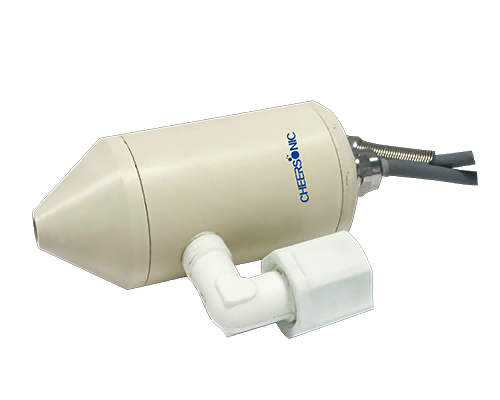
About Cheersonic
Cheersonic is the leading developer and manufacturer of ultrasonic coating systems for applying precise, thin film coatings to protect, strengthen or smooth surfaces on parts and components for the microelectronics/electronics, alternative energy, medical and industrial markets, including specialized glass applications in construction and automotive.
Our coating solutions are environmentally-friendly, efficient and highly reliable, and enable dramatic reductions in overspray, savings in raw material, water and energy usage and provide improved process repeatability, transfer efficiency, high uniformity and reduced emissions.
Chinese Website: Cheersonic Provides Professional Coating Solutions
