
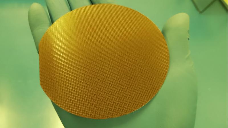
300mm Wafers Coated With 2um Photoresist
300mm Wafers Coated With 2um Photoresist – Ultrasonic Photoresist Coated – Cheersonic
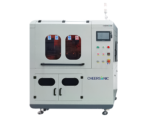
In the field of microelectronics manufacturing, the quality of photoresist coating on the substrate surface directly affects the performance and yield of devices, especially for devices with complex microstructures. Traditional spraying techniques often face problems such as uneven coating, material waste, and poor coverage of complex morphologies. The emergence of ultrasonic spray photoresist technology provides an efficient solution for the precise coating requirements of MEMS (Micro Electro Mechanical Systems) wafers and various substrates with different morphologies, effectively breaking through the technical bottleneck of traditional processes.
The core advantage of ultrasonic spraying technology lies in its unique atomization principle. This technology uses high-frequency ultrasonic vibration (usually in the frequency range of 20kHz-100kHz) to act on photoresist liquid, causing the liquid to be atomized into small droplets with uniform diameter (droplet diameter can be controlled between 5 μ m-50 μ m) without pressure impact. Compared with traditional pressure spraying technology, its atomization process is gentler, avoiding problems such as droplet splashing and coating edge accumulation caused by high-pressure spraying. At the same time, the atomized droplets have excellent dispersibility and flowability, which can uniformly cover the substrate surface under the precise guidance of airflow. Even micro grooves, protruding structures, or irregular surfaces on the substrate can achieve complete coverage without dead corners, greatly improving the coating consistency of complex shaped substrates.
For MEMS wafers, their surfaces are usually integrated with a large number of micro – or even nano scale microstructures (such as grooves and cavities of microsensors and microactuators). Traditional spray coating techniques are prone to the phenomenon of thin coating at the bottom of grooves and thick coating at the top of protrusions during the coating process of such structures, which leads to a decrease in pattern transfer accuracy in subsequent photolithography processes and affects device functionality. Ultrasonic spraying technology, with its delicate atomization of droplets and precise spray control, can accurately fill the microstructure gaps of MEMS wafers by adjusting the spraying distance (usually controlled between 5cm-20cm), ultrasonic vibration frequency, and airflow velocity, while ensuring the flatness of the surface coating. For example, in MEMS wafer coatings with micro grooves ranging from 1 μ m to 5 μ m in depth, ultrasonic spraying technology can achieve a thickness deviation of the coating inside and outside the grooves within ± 5%, which is much better than the traditional technology’s deviation range of ± 15%, providing reliable guarantees for high-precision manufacturing of MEMS devices.
In addition to MEMS wafers, ultrasonic spray photoresist technology can also adapt to various substrate shapes such as ceramic substrates, flexible metal substrates, glass substrates, etc. Taking flexible metal substrates as an example, there may be slight wrinkles or curved structures on their surface. Traditional spraying techniques are prone to coating fracture or uneven thickness due to changes in substrate morphology. However, the atomized droplets of ultrasonic spraying have good adhesion and extensibility, and can adaptively adjust with the surface morphology of flexible substrates. On substrates with a bending angle not exceeding 30 °, the stability of coating thickness can still be maintained. For substrates with high surface roughness such as ceramic substrates, this technology optimizes atomization parameters to allow photoresist droplets to fully fill the small pores on the substrate surface, forming a continuous pinhole free coating, effectively improving the insulation performance and corrosion resistance of the coating.
In the field of large-scale substrate coating, ultrasonic spraying technology has also demonstrated significant advantages, especially in achieving precise coating of 2 μ m thickness photoresist on the surface of 300mm wafers. As the mainstream large-size substrate in the current semiconductor manufacturing field, the coating process of 300mm wafers requires extremely strict uniformity – the coating thickness deviation within the entire wafer range needs to be controlled within ± 0.1 μ m, otherwise it will cause differences in the lithography pattern between the wafer edge and the central area, affecting device consistency. Ultrasonic spraying technology utilizes a multi nozzle collaborative working mode, combined with a high-precision motion platform (positioning accuracy up to ± 1 μ m), to achieve precise spraying of 300mm wafer surfaces area by area. In the preparation of 2 μ m thin coatings, this technology precisely controls the deposition rate of atomized droplets (adjustable to 0.1 μ m/s-1 μ m/s), avoiding pinhole defects caused by thin coatings in traditional techniques, while significantly improving material utilization (from 30% -40% in traditional spraying to over 70%) and reducing manufacturing costs.
In addition, ultrasonic spray photoresist technology also has good process compatibility and flexibility. For photoresist with different viscosities, stable atomization can be achieved by adjusting the ultrasonic vibration frequency and liquid supply rate; At the same time, this technology can seamlessly integrate with automated production lines, and through real-time monitoring systems, online detection and parameter adjustment of coating thickness and uniformity can be carried out, further improving production efficiency and product yield. In the current trend of miniaturization and high integration of microelectronic devices, ultrasonic spray photoresist technology is becoming a key technology in MEMS manufacturing and multi type substrate coating processes, providing strong support for the high-quality development of the microelectronics industry, thanks to its outstanding advantages in complex morphology adaptation, large-scale precise coating, and efficient material utilization.
About Cheersonic
Cheersonic is the leading developer and manufacturer of ultrasonic coating systems for applying precise, thin film coatings to protect, strengthen or smooth surfaces on parts and components for the microelectronics/electronics, alternative energy, medical and industrial markets, including specialized glass applications in construction and automotive.
Our coating solutions are environmentally-friendly, efficient and highly reliable, and enable dramatic reductions in overspray, savings in raw material, water and energy usage and provide improved process repeatability, transfer efficiency, high uniformity and reduced emissions.
Chinese Website: Cheersonic Provides Professional Coating Solutions
