
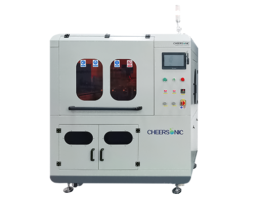
Spray Photoresist Coating Machine
With the continuous upgrading of semiconductor manufacturing processes, the limitations of traditional spin coating technology in controlling ultra-thin adhesive layers and coating complex surfaces are becoming increasingly prominent. The spray type photoresist coating machine, through technological innovation, has achieved precise control over the entire range from 50 nanometer ultra-thin coatings to thicker adhesive layers of over 30 microns, while solving the problem of uniform coating on high and low undulating surfaces, providing key support for advanced processes and 3D integration processes.
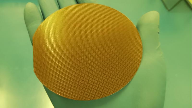
The core advantage of this device comes from the application of ultrasonic atomization spraying technology. Unlike traditional spin coating that relies on centrifugal force to form coatings, ultrasonic atomization breaks the photoresist into small droplets of uniform diameter (usually controlled below the micrometer level) through high-frequency vibration, and then precisely delivers them to the wafer surface through low-pressure carrier gas. This method not only allows the thickness of the photoresist to be controlled as thin as 50 nanometers, which is much lower than the lower limit of ArF photoresist thickness of 0.2-0.5 μ m in traditional spin coating technology, but also achieves high uniformity deposition of thicker photoresist layers of over 30 microns by adjusting parameters such as ultrasonic power and spraying path. Experimental data shows that the optimized ultrasonic spraying process can control the uniformity of film thickness at a lower level (the smaller the τ value, the better), meeting the strict requirements of precision lithography for coating consistency.
For structured wafer surfaces with undulations exceeding 50 microns, the equipment has achieved uniform coating through multi-dimensional process optimization. In typical three-dimensional structure coatings such as TSV (through silicon via), traditional spin coating is prone to forming thin adhesive at the bottom of the trench and edge accumulation due to centrifugal force, while ultrasonic atomization spraying improves through the following mechanisms: firstly, small droplets can penetrate deep into high aspect ratio structures with the help of nitrogen current, thereby improving step coverage; The second is to heat the carrier to quickly solidify the droplets upon reaching the surface, avoiding thickness deviation caused by gravity flow; The third is to compensate for the morphological differences in different areas by dynamically adjusting the nozzle spacing (usually optimized within 10-20 μ m) and scanning speed. A certain study shows that under the parameter combination of dilution mass ratio of 5:1 and ultrasonic power of 2kW, a coating with fine particles and uniform coverage can be obtained on the surface of TSV structure.
Ultrasonic atomization technology also brings significant advantages in process economy and environmental protection. In traditional spin coating processes, over 80% of photoresist is wasted due to centrifugal force, while ultrasonic spraying achieves a raw material utilization rate of over 90% through low-pressure delivery and precise deposition, significantly reducing organic material consumption. Meanwhile, its non-contact spraying method reduces mechanical damage to the wafer surface, and the titanium alloy nozzle is less prone to clogging and has low maintenance costs, making it suitable for large-scale production scenarios.
In terms of application scenarios, the device can cover diverse needs from advanced logic chips to MEMS sensors: in advanced processes below 7nm, the 50nm ultra-thin adhesive layer supports high-precision graphic transfer; In power device packaging, a 30 micron thick adhesive layer can meet the requirements of thick photoresist lithography; The adaptability to high and low undulating surfaces provides key process guarantees for the manufacturing of complex structures such as 3D IC stacks and microfluidic chips. This full scene adaptability makes it an important process equipment in the transition of semiconductor manufacturing from planar to three-dimensional architecture.
With the development of semiconductor devices towards high-density and three-dimensional, photoresist coating technology is upgrading from “planar uniformity” to “three-dimensional consistency”. The spray type photoresist coating machine combines ultrasonic atomization with intelligent process control, which not only breaks through the physical limitations of traditional technology, but also provides a new technological path for the sustainable development of the semiconductor manufacturing industry by improving material utilization and expanding process compatibility.
About Cheersonic
Cheersonic is the leading developer and manufacturer of ultrasonic coating systems for applying precise, thin film coatings to protect, strengthen or smooth surfaces on parts and components for the microelectronics/electronics, alternative energy, medical and industrial markets, including specialized glass applications in construction and automotive.
Our coating solutions are environmentally-friendly, efficient and highly reliable, and enable dramatic reductions in overspray, savings in raw material, water and energy usage and provide improved process repeatability, transfer efficiency, high uniformity and reduced emissions.
Chinese Website: Cheersonic Provides Professional Coating Solutions
