
Wafer Preparation Process
Wafer Preparation Process – Wafer Coating Process – Cheersonic
The ingot also undergoes a series of processing to form a semiconductor substrate, or wafer, that meets the requirements of semiconductor chip manufacturing.
Silicon is the most important semiconductor material in integrated circuit manufacturing, and more than 90% of integrated circuit chips are fabricated on silicon wafers. The preparation process of silicon single crystal polished wafers is relatively complicated, and the processing steps are many and long. The processing quality of each process must be strictly controlled to obtain silicon single crystal polished wafers that meet the technical requirements of integrated circuits and are of qualified quality.
Wafer preparation has the following steps
1. Truncation
Truncation refers to the removal of both ends of the silicon rod. The two ends are usually called the seed crystal end and the non-seed crystal end. This is because the impurity content at both ends of the crystal rod is quite different from the middle, and the diameter of the two ends is smaller than In the middle, in order to obtain wafers of the same diameter in the subsequent process, it must be cut off.
2. Radial tumbling
Since the control of diameter and roundness in crystal growth cannot be very precise, the silicon rods must be grown slightly larger for radial grinding. Tumble grinding is usually performed on a centerless tumbling mill to obtain precise diameter single crystal silicon, and wafer warpage and breakage are reduced through tight diameter control.
3. Grinding the positioning surface
Single crystal has the characteristics of anisotropy. It must be cut according to a specific crystal orientation to meet the needs of production, and it will not be broken, so it should be oriented before cutting. With the development of integrated circuit manufacturing technology for semiconductor devices, the size of the wafers used is increasing day by day. If the chip is divided along the cleavage plane, the cleavage part is relatively flat and easy to crack, and the chip of the chip is less, thereby reducing the scratch of the chip aluminum strip and the damage rate of the die during dicing.
The principle of orientation is to use a beam of visible light or X-ray to shoot the end face of the single crystal rod. Due to the different crystal orientations on the end face, the reflected pattern is also different. From the reflection image, the crystal orientation of the single crystal rod can be corrected.
Once the crystal is oriented on the cutting block, roll a reference plane along the axis as shown.
In many crystals, the edge has a second, smaller reference plane, called the sub-reference plane, that differentiates the conductivity type. The angle of the primary and secondary positioning edges identifies the type of silicon wafer.
4. Slicing
After the shape of the ingot is processed, directional slicing is performed, and the wafer is cut from the crystal with a diamond-coated circular blade.
Single crystal silicon is cut into silicon wafers, usually using an inner circle slicer or a wire slicer. The inner circle slicer adopts a high-strength rolled ring-shaped steel plate blade. The outer ring is fixed on the runner, and the blade is tightened. The inner edge of the ring has hard granular diamonds. The shape of the inner circle slicer is shown in the figure below. When slicing, the blade rotates at a high speed, and under the action of the coolant, the monocrystalline silicon fixed on the graphite strip will move relative to the blade.
This cutting method has mature technology, good blade stability, good wafer surface flatness, relatively cheap equipment and easy maintenance. However, because the blade has a certain thickness, about 250 and 300 microns, about one-third of the crystals will become sawdust during the slicing process, and the inner circle slicing speed is slow and the efficiency is low.
Another slicing method is wire slicing, which is achieved by the movement of a wire with diamond particles attached to it. The use of wire slicers started in 1995, and the output of one money slicer is equivalent to 35 internal circular slicers. Usually the metal diameter of the money slice is only 180 microns. For the same single crystal silicon, the wire slicer can reduce the material loss by about 25%, and the stress of the wire slice is small, and the surface damage of the silicon wafer after slicing is small. However, the flatness of the silicon wafer is slightly poor, the equipment is relatively expensive, and maintenance is difficult. Monocrystalline silicon wafers for solar cells do not have high requirements on the flatness of the wafers, so wire slicers are more suitable for slicing monocrystalline silicon for solar cells.
5. Grinding
After the slicing is completed, the surface of the silicon wafer is subjected to grinding and machining. The purpose of the grinding process includes the following two points.
①Remove the scar on the surface of the silicon wafer, so that the surface processing damage of the silicon wafer is uniform.
②Adjust the thickness of the silicon wafer, so that the thickness between the wafers is gradually reduced, and the surface flatness and parallelism are improved.
6. Chamfer
Chamfering is to use a specially shaped grinding wheel to remove sharp chipping, edges and cracks on the edge of the silicon wafer. Chamfering can be done before or after grinding. There are three main purposes of chamfering.
① Prevent wafer edge cracking.
②Prevent the concentration of thermal stress.
③ Increase the flatness of the epitaxial layer and the photoresist layer at the edge of the wafer.
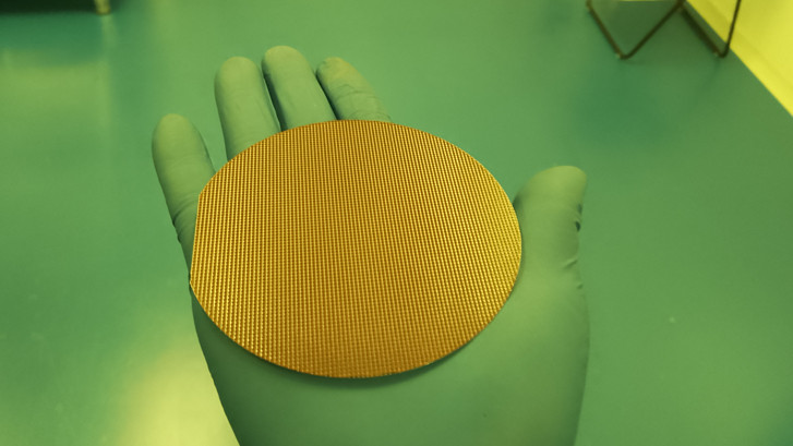
7. Polished
Polishing is the last important processing step on the surface of the silicon wafer, and it is also the most delicate surface processing. The purpose of polishing is to remove the fine damage layer on the surface and obtain a smooth surface with high flatness.
Ultrasonic spraying technology is used for semiconductor photoresist coating. Compared with traditional coating processes such as spin coating and dip coating, it has the advantages of high uniformity, good encapsulation of microstructures, and controllable coating area. In the past 10 years, it has been fully demonstrated that the 3D microstructure surface photoresist coating using ultrasonic spraying technology, the prepared photoresist coating is significantly higher than the traditional spin coating in terms of microstructure wrapping and uniformity Craft.
The ultrasonic spraying system can precisely control the flow rate, coating speed and deposition volume. Low-speed spray shaping defines atomized spray as a precise and controllable pattern to avoid excessive spray when producing a very thin and uniform layer. The ultrasonic spray system can control the thickness from sub-micron to more than 100 microns, and can coat any shape or size.
