
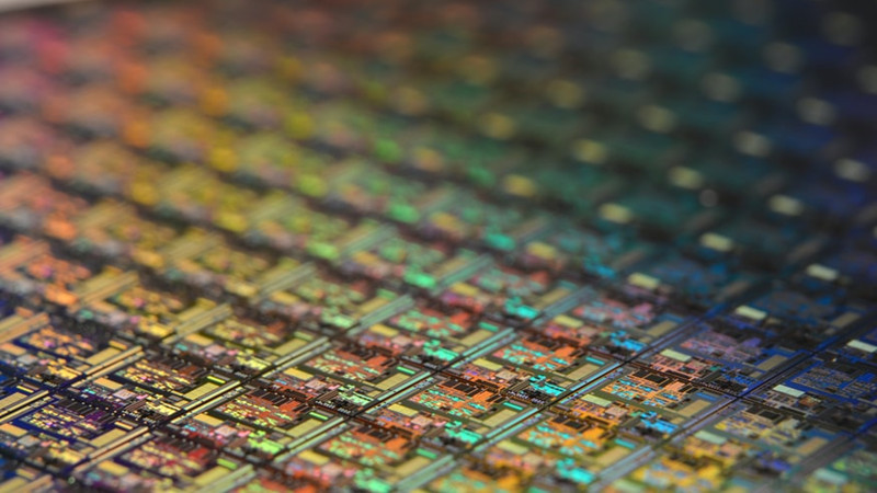
Wafer Fabrication Etching Technology
Wafer Fabrication Etching Technology – Semiconductor Coating Systems – Cheersonic
Dry etching is the most important surface material removal method in chip manufacturing, with better profile control. The dry etching method is divided into physical etching, chemical etching and physical and chemical comprehensive action etching according to the mechanism of action. In the combined mechanism of physics and chemistry, the physical process of ion bombardment can remove surface materials by sputtering, which has strong directionality. Ion bombardment can improve chemical etching, allowing reactive elements to react more efficiently with silicon surface species. The comprehensive dry etching method combines the advantages of ion sputtering and surface reaction, so that the etching has better selectivity ratio and line width control.
Various types of dry etching processes are required in the fabrication of integrated circuits, with applications involving various materials on silicon wafers. The materials to be etched mainly include dielectrics, silicon and metals, etc. By cooperating with lithography, deposition and other processes for many times, a complete underlying circuit, gate, insulating layer and metal path can be formed.
Dry etching of dielectrics mainly includes oxide etching and silicon nitride etching, and is the most complicated etching process. The oxide is usually etched to make contact holes and vias. High aspect ratio windows are required to be etched in oxide, typically using fluorocarbon chemistries. Commonly used gases for etching of silicon nitride are, and mixed with and used.
Plasma dry etching of silicon is a key process technology in the manufacture of silicon wafers. The structure of the polysilicon gate has high requirements for etching, and must have a high selectivity ratio to the underlying gate oxide layer and have very good uniformity and repeatability. Fluorine-based gases are generally used for polygate etching. Monocrystalline silicon etching is primarily used to create trenches, requiring each trench to maintain a consistent finish, close vertical sidewalls, correct depth, and rounded trench top and bottom corners. Fluorine gas is used for etching of shallow grooves, which has a high selectivity ratio to photoresist. Chlorine-based or bromine-based gases are often used for deep groove etching, which has a high etching rate and a high selectivity ratio for silicon oxide.
Metal etching is mainly used in metal interconnect lines, through holes, contact metals and other links. Metal interconnects are usually made of aluminum alloys, which are etched with chlorine-based gases and some polymers. Tungsten is often used as a filler for vias in multilayer metal structures, usually with fluorine- or chlorine-based gases.
The ultrasonic coating system can use advanced layering technology to precisely control the flow rate, coating speed and deposition amount. Low-speed spray forming defines an atomizing spray as a precise, controllable pattern, avoiding excessive spraying when producing very thin and uniform layers. It turns out that direct spraying using ultrasonic technology is a reliable and effective way to deposit photoresist on 3D microstructures, thereby reducing equipment failures caused by excessive metal exposure to etchant.
Ultrasonic spray systems have proven to be suitable for a variety of applications that require uniform, repeatable photoresist or polyimide film coatings. Cheersonic’s coating system can control thicknesses from sub-micron to more than 100 microns, and can coat any shape or size. It is a feasible alternative to other coating technologies such as spin coating and traditional spray coating.
Cheersonic’s non-blocking ultrasonic coating technology is known for its ultra-thin micron-layer coatings of functional and protective materials. The ultrasonic vibration of the nozzle effectively dispersed the particles in the suspension and produced a very uniform particle dispersion in the film layer, while the conductive particles did not settle out of the suspension.
