
Ultrasonic Spraying Coating Transparent Conductive Film
Ultrasonic Spraying Coating Transparent Conductive Film – Cheersonic
In today’s era of rapid development in flexible electronics, optoelectronic displays, and new energy industries, transparent conductive films, as a key functional material, directly determine the performance of related devices in terms of their properties and preparation processes. Traditional film making methods such as spin coating, scraping coating, or vapor deposition are either limited by material utilization or difficult to achieve uniform coverage on large-area substrates, and appear inadequate when facing flexible or irregular substrates. Ultrasonic spraying technology, as an emerging precision deposition process, provides a highly promising technological path for the preparation of high-performance transparent conductive films with its unique advantages.
Technical core: Working principle and essence of ultrasonic spraying
The core of ultrasonic spraying technology lies in its “ultrasonic atomization” mechanism. Different from the traditional pneumatic spray that relies on high-pressure gas to break liquid, ultrasonic spraying equipment converts high-frequency electric energy into mechanical vibration through piezoelectric transducer, which is transmitted to the nozzle tip, so that the spraying liquid (such as nano material dispersion liquid) flowing through can form extremely fine capillary waves on the surface, and finally be “torn” into uniform, micro and even nano scale droplets due to huge acceleration.
This principle brings several fundamental advantages:
1. Uniform and controllable fog droplets: The size distribution range of the generated fog droplets is extremely narrow, ensuring that the material amount at each “point” during the deposition process is highly consistent, which is the basis for achieving high uniformity of the film.
2. Low speed and weak impact: the droplets only rely on their own inertia and slight carrier gas to guide them to the substrate, and their kinetic energy is far lower than that of pneumatic spray. This means that it has minimal impact on the already formed underlying thin film or structurally precise substrate (such as nanowire networks), effectively avoiding the “scouring effect” and structural damage.
3. Extremely high material utilization rate: The spraying path and range can be precisely controlled by the program, and almost all atomized materials can be guided to the effective area of the substrate, with a utilization rate of over 90%, which is crucial for expensive nanomaterials such as silver nanowires.
Material System: An Ideal Deposition Platform for Diversified Transparent Conductive Materials
The mild and uniform characteristics of ultrasonic spraying make it an ideal choice for depositing various emerging transparent conductive materials, perfectly adapting to a diversified material system beyond traditional indium tin oxide.
1. Silver nanowires: As the most promising alternative material to ITO, silver nanowires achieve conductivity by interweaving into a network, while the pores between the networks ensure high transparency. However, spin coating method is prone to uneven orientation and stacking of nanowires due to centrifugal force; The scraping method is sensitive to the length of the line and can easily cause agglomeration. Ultrasonic spraying technology, with its low kinetic energy droplets, can evenly “sprinkle” silver nanowire dispersion on the substrate. The nanowires naturally settle and overlap under the surface tension of the solvent, forming a conductive network with better connectivity and fewer defects, thereby achieving higher light transmittance or lower resistance under the same light transmittance.
2. Carbon nanotubes: Single walled or multi walled carbon nanotubes also rely on the formation of a permeable network to conduct electricity. Ultrasonic spraying not only achieves uniform distribution of CNTs, but also helps to orient and arrange carbon nanotubes to a certain extent during deposition, reducing high contact resistance caused by disordered entanglement. Meanwhile, by layer by layer spraying or blending spraying with other materials, the network voids can be effectively filled, improving the density and conductivity uniformity of the film.
3. PEDOT: PSS (water-based conductive polymer dispersion): This type of material is known for its excellent flexibility, solution processability, and high transparency. However, during the film-forming process, the conductivity of PEDOT: PSS is highly susceptible to the influence of film-forming morphology and phase separation degree. Ultrasonic spraying can promote the formation of microstructures that are more conducive to charge transfer between PEDOT and PSS by precisely controlling the drying process of droplets. In addition, researchers often use ultrasonic spraying for secondary treatment, such as spraying a post-treatment solution of trace solvents (such as ethylene glycol, dimethyl sulfoxide) on PEDOT: PSS films, optimizing the film through precise dose control, significantly improving its conductivity without damaging the integrity of the film.
More importantly, ultrasonic spraying technology provides unprecedented convenience for the composite and stacking of the above-mentioned materials. It is easy to achieve the sequential deposition of “sandwich” structures (such as CNT/PEDOT: PSS/AgNW), or directly blend different material dispersions and spray them in one go, using synergistic effects to prepare composite transparent electrodes with superior comprehensive performance (conductivity, transparency, flexibility, stability).
Technological advantage: the key to moving towards industrial production
From laboratory to large-scale production, ultrasonic spraying technology has demonstrated its strong process adaptability.
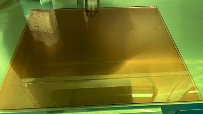
* Excellent uniformity and consistency: Whether it is small-sized silicon wafers or large glass substrates with diagonal lengths exceeding one meter, ultrasonic spraying can ensure astonishing consistency in film thickness and resistance, and the difference between on-chip and on-chip can be controlled at an extremely low level.
* Unparalleled patterning capability: Combined with a mask plate or directly linked to a motion platform, ultrasonic spraying can easily achieve complex and precise patterned deposition without the need for subsequent material reduction processes such as laser etching, avoiding material waste and potential structural damage. This is crucial for applications such as electrode circuits for touch screens and fine metal grids for OLEDs.
* Wide substrate adaptability: Its mild deposition characteristics enable it to cope with rigid glass, flexible PET/PC/PEN plastic films, and even special substrates such as paper and textiles that are not resistant to high temperatures and impacts, greatly expanding the application scenarios of transparent electrodes.
* Precision adjustable process parameters: atomization frequency, flow rate, distance between nozzle and substrate, movement speed, substrate temperature and many other parameters can be independently and accurately controlled, providing a huge “parameter space” for optimizing thin films in different materials and application scenarios, and helping to develop thin film products with performance limits.
Application prospects and future prospects
Based on the above advantages, transparent conductive films prepared by ultrasonic spraying technology have shown great potential in many cutting-edge fields:
* Flexible display and touch: providing bend resistant and highly reliable transparent electrodes for foldable and rollable display devices.
* Organic photovoltaics and perovskite solar cells: As the top or bottom electrode of the cell, efficient and low-cost solution preparation can be achieved, especially suitable for future large-scale roll to roll production processes.
* Transparent heating film: can be used to prepare car windshields, airplane portholes, or smart home panels with fast response and uniform heating.
* Electromagnetic shielding layer: provides lightweight and transparent electromagnetic interference protection inside flexible electronic devices.
Looking ahead to the future, with the advancement of nano material dispersion technology and the further improvement of automation and intelligence level of ultrasonic spraying equipment, this technology is expected to become the mainstream process in the field of transparent conductive film manufacturing. It will not only be a deposition tool, but also a comprehensive platform integrating material synthesis, structural control, and performance optimization, continuously promoting innovation and transformation of the next generation of optoelectronic devices.
About Cheersonic
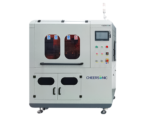
Cheersonic is the leading developer and manufacturer of ultrasonic coating systems for applying precise, thin film coatings to protect, strengthen or smooth surfaces on parts and components for the microelectronics/electronics, alternative energy, medical and industrial markets, including specialized glass applications in construction and automotive.
Our coating solutions are environmentally-friendly, efficient and highly reliable, and enable dramatic reductions in overspray, savings in raw material, water and energy usage and provide improved process repeatability, transfer efficiency, high uniformity and reduced emissions.
Chinese Website: Cheersonic Provides Professional Coating Solutions
