
Ultrasonic Atomization Spray in Thin-Film Photovoltaics
Process Application of Ultrasonic Atomization Spray in Thin-Film Photovoltaics – Cheersonic
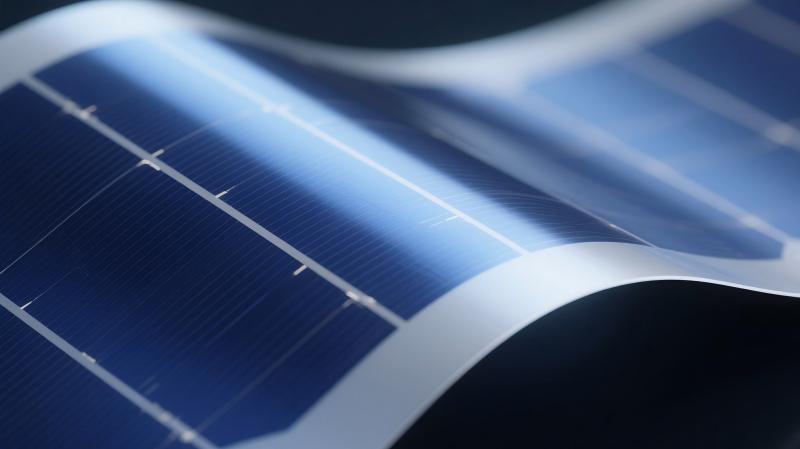
In the R&D and manufacturing of thin-film photovoltaic technologies, achieving efficient, uniform, and large-area repeatable thin-film deposition has long been one of the core challenges. Based on its unique atomization mechanism and mild deposition characteristics, ultrasonic atomization spray technology (often referred to as ultrasonic spray systems) is being widely adopted in the preparation of various thin-film photovoltaic material systems, demonstrating remarkable advantages especially in the processing of active layers and perovskite layers (including single-junction and tandem structures).
1. Precision Deposition of Active Layers
The active layer of thin-film photovoltaic devices is the core region for light absorption and charge generation. Its micro-morphology, thickness uniformity, and crystalline quality directly determine the photoelectric conversion efficiency of the cell.For material systems such as Copper Indium Gallium Selenide (CIGS), Cadmium Telluride (CdTe), and Organic Photovoltaics (OPV), traditional solution coating methods (e.g., spin-coating, blade-coating) often struggle to balance uniformity and material utilization on large-area substrates.Ultrasonic atomization spray technology breaks the precursor solution into micro- or even sub-micro-sized fine droplets, which are then guided by carrier gas onto the heated substrate surface, forming dense, pinhole-free wet films.In this process, the momentum of droplets is extremely low, avoiding impact damage to the pre-deposited film caused by high-speed jetting, while significantly reducing splashing and material waste.More importantly, this technology has high tolerance to physical properties such as solution viscosity and solid content, allowing researchers to flexibly formulate active layer recipes — for instance, organic photoactive mixtures with optimized donor-acceptor ratios, or CIGS precursor solutions doped with alkali metal elements — without frequent adjustments to deposition parameters.By precisely controlling droplet size, atomization flow rate, and substrate temperature, accurate thickness regulation from tens of nanometers to several micrometers can be realized, which is critical for optimizing the balance between light absorption and carrier transport.
2. Customized Coating of Perovskite Layers
The efficiency breakthroughs of perovskite solar cells in recent years have attracted considerable attention. For both conventional n-i-p and inverted p-i-n structures, the quality of polycrystalline perovskite films is key to device performance.In single-junction perovskite cells, depositing perovskite precursor solutions via ultrasonic atomization spray effectively promotes rapid solvent evaporation and uniform nucleation, yielding perovskite films with large grain size, low defect density, and high coverage.Unlike spin-coating, which relies on centrifugal force from substrate rotation, atomization spray is a non-contact, shear-stress-free coating method, particularly suitable for forming uniform wet films on rough or flexible substrates.By optimizing the relative motion trajectory between the atomization nozzle and the substrate, this technology can be easily scaled up to square-meter production dimensions while maintaining film thickness variation within 5%.Furthermore, in post-deposition passivation of perovskite layers, this technique can be used to deposit ultra-thin interface modification layers (e.g., organic ammonium salts or polymers), with precise control over sub-nanometer equivalent thickness, effectively passivating grain boundaries and surface defects.
3. Challenges of Multi-Layer Integration in Tandem Devices
For single-junction/tandem (or all-perovskite tandem) photovoltaic devices pursuing higher efficiencies, the structure typically incorporates multiple functional layers — such as bottom narrow-bandgap sub-cells (e.g., Sn-Pb mixed perovskite or silicon heterojunction), intermediate recombination or tunneling layers, and top wide-bandgap sub-cells (e.g., Br-rich perovskite).In this complex stacked architecture, deposition of each layer must not damage the underlying layers.The “soft landing” characteristic of ultrasonic atomization spray stands out here: owing to small droplet size and low velocity, secondary spraying onto surfaces already coated with sensitive organic hole transport layers or labile perovskite bottom cells does not cause re-dissolution or morphological damage to the lower layers.Meanwhile, the technology enables precise control over the precursor composition of each layer — such as adjusting the Br/I ratio in top wide-bandgap perovskite, or incorporating Sn in bottom narrow-bandgap layers to reduce the bandgap — without cross-contamination between different solutions.More importantly, in fabricating all-perovskite tandem cells, the thickness, crystallographic orientation, and defect distribution of top and bottom perovskite layers require synergistic optimization.By independently tuning atomization parameters (e.g., ultrasonic power, solution flow rate, substrate temperature) for each sub-cell coating step, optical absorption and electrical transport properties optimal for each sub-bandgap can be separately achieved, enabling conversion efficiencies exceeding the single-junction Shockley-Queisser limit.
4. Process Compatibility and Future Outlook
Beyond the above core applications, this spray technology is also widely used in preparing electron transport layers (e.g., SnO₂, TiO₂) and hole transport layers (e.g., Spiro-OMeTAD, PTAA), and even for depositing catalytic seed layers for metal electrodes.Its open, in-line adjustable nature allows seamless scale-up from lab-scale formulation development to roll-to-roll or sheet-to-sheet mass production lines.In the future, with the continuous maturation of perovskite/silicon, perovskite/perovskite, and perovskite/CIGS tandem technologies, higher demands will be placed on thickness uniformity (especially sub-nanometer variation over large areas) and interface purity of each thin film.With advantages including high material utilization (typically >90%), ease of fabricating gradient-composition films, and compatibility with both high- and low-boiling-point solvent systems, ultrasonic atomization spray systems are expected to become an indispensable process module in next-generation high-efficiency, stable, and large-area manufacturable thin-film photovoltaic platforms.Notably, in practical applications, spray parameters must be finely optimized for specific perovskite recipes (e.g., anti-solvent engineering, annealing strategies). Nevertheless, the inherent flexibility and controllability of this technology have already provided a solid engineering foundation for manufacturing photovoltaic devices ranging from single-junction to complex multi-junction structures.
About Cheersonic
Cheersonic is the leading developer and manufacturer of ultrasonic coating systems for applying precise, thin film coatings to protect, strengthen or smooth surfaces on parts and components for the microelectronics/electronics, alternative energy, medical and industrial markets, including specialized glass applications in construction and automotive.
Our coating solutions are environmentally-friendly, efficient and highly reliable, and enable dramatic reductions in overspray, savings in raw material, water and energy usage and provide improved process repeatability, transfer efficiency, high uniformity and reduced emissions.
Chinese Website: Cheersonic Provides Professional Coating Solutions
