
Silicon Wafers and Microneedles
Ultrasonic spraying technology is showing irreplaceable advantages in modern micro nano manufacturing, especially in the field of photoresist coating for precision components such as silicon wafers and microneedles.
For silicon wafers, traditional spin coating methods can easily lead to edge accumulation, material waste, and poor uniformity when processing large-sized, irregular, or textured wafers. Ultrasonic spraying utilizes high-frequency vibration to atomize photoresist solution into micrometer sized uniform particles, which are then sprayed onto the wafer surface through precisely controlled nozzles. This method can achieve high uniformity coating with nanoscale thickness, greatly saving expensive photoresist and perfectly adapting to the complex structure coating of future 3D integrated chips.
On more challenging microneedle arrays, the high aspect ratio and three-dimensional structure of microneedles make it almost impossible to achieve complete coverage through spin coating. Ultrasonic spraying, with its soft “soft mist” characteristics, can wrap around the tip and sidewall of each microneedle without dead corners, forming a complete, uniform, and defect free adhesive film, laying a solid foundation for subsequent micro nano graphic processing.
Therefore, ultrasonic spraying technology, with its excellent uniformity, high material utilization rate, and outstanding adaptability, is driving the semiconductor and MEMS fields towards a more precise and efficient direction.
Spraying photoresist onto three-dimensional structures like silicon wafers and microneedles presents distinct characteristics and challenges. The following is a related analysis:
Spraying photoresist onto silicon wafers:
Advantages:
- High flatness and uniformity: Silicon wafers have a highly flat surface. Using conventional processes like spin coating, photoresist can be evenly applied to the wafer surface, forming a uniform film thickness. This is crucial for accurate light illumination and precise pattern transfer in subsequent photolithography processes. For example, in large-scale integrated circuit manufacturing, a uniform photoresist layer ensures consistent size and performance across all transistors on the chip.
- Good adhesion: The surface properties of silicon wafers are highly compatible with photoresist. After proper surface treatment, the photoresist adheres firmly to the wafer and resists removal during subsequent cleaning and etching processes, ensuring process stability and reliability.
- Easy to mass-produce: Silicon wafers have a high degree of dimensional standardization, making them suitable for large-scale automated production equipment. In semiconductor manufacturing plants, automated coating equipment can quickly and accurately spray photoresist onto silicon wafers, improving production efficiency and product quality.
Challenges:
- Particle contamination control: When spraying photoresist onto silicon wafers, particle contamination in the environment must be strictly controlled. Even tiny particles adhering to the photoresist layer can cause pattern defects during the subsequent photolithography process, affecting chip performance. Therefore, the coating process typically requires extremely clean rooms.
- Precise thickness control: With the continuous advancement of semiconductor technology, chip line widths are becoming increasingly smaller, and the requirements for photoresist thickness precision are also becoming increasingly stringent. Precise control of parameters such as the spray volume and rotation speed is required to ensure that the thickness of the photoresist layer meets the design requirements.
Spraying photoresist onto three-dimensional structures such as microneedles:
Advantages:
- Good adaptability: For microneedles with complex three-dimensional structures, spray coating technology can flexibly adapt to their shape and size, achieving comprehensive coverage. Whether it’s the microneedle tip, body, or base, the photoresist can be evenly applied to the surface by adjusting the spraying angle and parameters, providing a good pattern foundation for subsequent microfabrication processes.
- High-precision patterning: Utilizing the photosensitivity of photoresist, the desired pattern can be precisely formed on the microneedle. For example, after spraying photoresist on the microneedle tip, photolithography can be used to create tiny holes or grooves for applications such as drug delivery or biosensing.
- Multi-layer spraying: For microneedle devices requiring a multi-layer structure, this can be achieved through multiple sprayings of photoresist. Each layer of photoresist can be designed and processed differently as needed, creating complex three-dimensional microstructures.
Challenges:
- Difficulty in uniformity control: Compared to flat silicon wafers, the three-dimensional structure of microneedles has a larger surface area and complex shape, making it difficult to achieve uniform distribution of photoresist during the spraying process. Photoresist accumulation or incomplete coverage is common on sharp, curved, or narrow gaps of microneedles. Optimizing the spray coating process and equipment is crucial to improve photoresist uniformity.
- Adhesion Issues: Microneedles often have high surface roughness or special materials, which can affect photoresist adhesion. Before spray coating, the microneedle surface requires appropriate treatment, such as cleaning and activation, to enhance the bond between the photoresist and the microneedle surface. Furthermore, care must be taken to prevent photoresist detachment or deformation during subsequent processing.
- Increased Process Complexity: The three-dimensional structure of microneedles and the unique requirements of photoresist increase the complexity of the entire spray coating and photolithography process. Precise control of spray coating parameters, photolithography exposure time, and development conditions is required to ensure pattern accuracy and quality. Furthermore, customized process design and optimization are required for microneedles of varying shapes and sizes, increasing the difficulty and cost of process development.
About Cheersonic
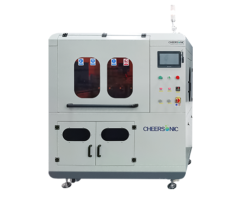
Cheersonic is the leading developer and manufacturer of ultrasonic coating systems for applying precise, thin film coatings to protect, strengthen or smooth surfaces on parts and components for the microelectronics/electronics, alternative energy, medical and industrial markets, including specialized glass applications in construction and automotive.
Our coating solutions are environmentally-friendly, efficient and highly reliable, and enable dramatic reductions in overspray, savings in raw material, water and energy usage and provide improved process repeatability, transfer efficiency, high uniformity and reduced emissions.
Chinese Website: Cheersonic Provides Professional Coating Solutions
