
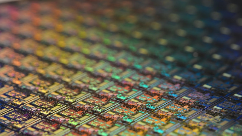
Semiconductor Wafer Manufacturing Process
Semiconductor Wafer Manufacturing Process – Semiconductor Coatings – Cheersonic
The manufacturing process of semiconductor silicon wafers is complex, and single crystal pulling is the key link
The upstream of semiconductor wafers is semiconductor-grade polysilicon material, and the downstream is semiconductor products. Silicon is the main form of silicon dioxide in nature, and it is chemically reduced to generate polysilicon material, and then purified. The purity requirements of polysilicon materials for photovoltaics are between 6 and 9 “9” (99.9999%-99.9999999%), and the purity of semiconductor materials requires more than 11 “9” (99.999999999%). The fabricated semiconductor wafers are used as substrates in wafer factories to manufacture various semiconductor products, which are ultimately used in terminal products such as mobile phones and computers.
The manufacturing process of semiconductor silicon wafers is complex, mainly including processes such as pulling single crystals and cutting, grinding, polishing and epitaxy of silicon wafers. The production process of semiconductor silicon wafers is complex and involves many processes. The grinding sheet process includes pulling single crystal, truncating, spheronizing, slicing, chamfering, grinding, etc. The polishing sheet is manufactured on the basis of the grinding sheet through edge polishing, surface polishing and other processes; The silicon annealed sheet is produced by annealing heat treatment, and the silicon-on-insulator SOI is produced by a special process. Silicon wafers need to be cleaned many times during the manufacturing process, and they also need to be inspected and packaged before being sold to customers.
Step 1: Pull the single crystal. Electronic-grade high-purity polysilicon can be drawn into single-crystal silicon rods through a single-crystal growth process. Commonly used methods include Czochralsk (CZ) and Float-Zone (FZ). The FZ method has high purity, low oxygen content, high resistivity, and can withstand high pressure, but the process is difficult, the preparation of large-sized silicon wafers is difficult and the cost is high, so it is mainly 8 inches and below, mainly used for high-end power devices. . The CZ method has high oxygen content, it is easier to produce large-sized single crystal silicon rods, the technology is mature, and the cost is low. Therefore, the current semiconductor industry mainly uses the CZ method to draw single crystal silicon rods. The single crystal pulling technology directly determines the density of crystal primary defects such as dislocation, COP (crystal originated pit, crystal primary pit), vortex, and the quality of crystal technical indicators such as resistivity, resistivity gradient, oxygen, and carbon content. The most core technology in the semiconductor wafer production process.
Czochralski processing technology:
Charging: Put polysilicon and dopant into the quartz crucible in the single crystal furnace. The type of dopant depends on the resistivity required to grow, mainly including boron for growing P-type and phosphorus and arsenic for growing N-type. , Antimony, etc.
Melting: After charging, heat to above the melting temperature of silicon (1420℃), melt the polysilicon and dopant, and after volatilizing for a certain period of time, lower the seed crystal to the liquid level, and preheat the seed crystal for a few minutes, commonly known as “” Baked crystals” to remove surface volatile impurities and reduce thermal shock.
Seeding: When the temperature is stable, the seed crystal is brought into contact with the melt, and then the seed crystal with a certain speed is lifted up at a certain speed. As the seed crystal rises, silicon crystallizes at the head of the seed crystal, which is called “seeding” or “seeding”. sow”.
Necking: Slightly lower the temperature after seeding, increase the pulling speed, and pull a section with a smaller diameter than the seed crystal. The purpose is to eliminate polycrystals caused by poor contact and try to eliminate the extension of original dislocations in the seed crystals. The neck is generally longer than 20 mm.
Shouldering: After the necking process is completed, the diameter of the crystal is gradually increased to the required diameter by gradually reducing the lifting speed and adjusting the temperature. It can be judged whether the crystal is a single crystal when the shoulder is placed, otherwise it should be melted and re-seeded.
Equal diameter growth: When the crystal diameter reaches the required size, increase the pulling speed so that the crystal diameter will not increase, which is called shouldering. Keeping the crystal diameter unchanged after shouldering is equal diameter growth. At this time, the temperature and pulling speed should be strictly controlled. Monocrystalline silicon wafers are taken from equal diameter sections.
Finishing: If the ingot is separated from the liquid surface immediately after the length of the equal diameter section, the effect of stress will cause dislocations and slip lines to appear in the ingot. Therefore, in order to avoid this problem, the diameter of the ingot must be gradually reduced until it becomes a sharp point and is separated from the liquid surface.
District melting method:
Step 1: In a furnace chamber under a vacuum or rare gas environment, use an electric field to heat the polycrystalline silicon rod until the polycrystalline silicon in the heated area is melted to form a melting area. The molten zone is contacted with the seed crystal and melted. The melting zone on the polycrystalline silicon is continuously moved upwards, while the seed crystals are slowly rotated and stretched downwards to gradually form monocrystalline silicon rods.
Step 2: Slice. The single crystal silicon rod is ground to the same diameter, and then according to the resistivity required by the customer, the crystal rod is cut into about 1 mm thick slices with an inner diameter saw or a wire saw to form a wafer. According to the current process and technical level, in order to reduce the loss of silicon material, improve the production efficiency and surface quality, the wire cutting method is generally used for slicing.
Step 3: Chamfering: The purpose of chamfering of silicon wafers is to eliminate edges, cracks, burrs, chipping or other defects and various edge surface contaminations generated by cutting the edge surface of silicon wafers, thereby reducing the edge surface of silicon wafers. The roughness of the silicon wafer increases the mechanical strength of the edge surface of the silicon wafer and reduces the surface contamination of the particles.
Step 4: Grinding. Use abrasives on a grinder to polish the slices to the desired thickness while improving surface flatness. The purpose of grinding is to remove the surface mechanical stress damage layer with a depth of about 20~25 μm and various metal ions on the surface of the silicon wafer during the slicing process, and to make the silicon wafer have a certain flat surface. .
Step 5: Etching and Polishing. The mechanical damage to the wafer surface caused by the previous steps is removed by chemical etching, and then the silicon sol mechanochemical polishing method is used to make the wafer surface more flat and smooth.
Step Six: Cleaning and Inspection. After cleaning, the products are subject to strict quality inspection, and are sold to customers after being qualified. It can also be further used to make special silicon wafers such as SOI and epitaxial wafers.
The ultrasonic coating system can use advanced layering technology to precisely control the flow rate, coating speed and deposition amount. Low-speed spray forming defines an atomizing spray as a precise, controllable pattern, avoiding excessive spraying when producing very thin and uniform layers. It turns out that direct spraying using ultrasonic technology is a reliable and effective way to deposit photoresist on 3D microstructures, thereby reducing equipment failures caused by excessive metal exposure to etchant.
Ultrasonic spray systems have proven to be suitable for a variety of applications that require uniform, repeatable photoresist or polyimide film coatings. Cheersonic’s coating system can control thicknesses from sub-micron to more than 100 microns, and can coat any shape or size. It is a feasible alternative to other coating technologies such as spin coating and traditional spray coating.
Cheersonic’s non-blocking ultrasonic coating technology is known for its ultra-thin micron-layer coatings of functional and protective materials. The ultrasonic vibration of the nozzle effectively dispersed the particles in the suspension and produced a very uniform particle dispersion in the film layer, while the conductive particles did not settle out of the suspension.
