
Semiconductor Photoresist
Semiconductor Photoresist – Lithography Coating – Cheersonic
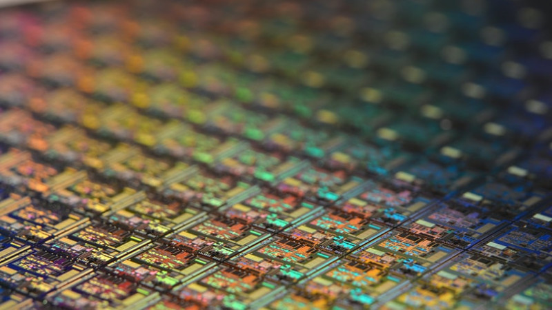
Photoresist, also known as photoresist, refers to a resist etching film material whose solubility changes through irradiation or radiation of ultraviolet light, electron beam, ion beam, X-ray, etc., mainly composed of photoresist resin, It is composed of sensitizer (photoinitiator + photosensitizer + photoacid generator), monomer, solvent and other auxiliaries. Due to many application scenarios, photoresists for different purposes have different performance requirements such as exposure light source, manufacturing process, film-forming characteristics, etc., as well as different requirements for material solubility, etching resistance and photosensitivity, and the proportion of different raw materials will be different. A very large change, in which the photoresist resin is the main component of the photoresist, and the cost accounts for 50%. Photoresist is an extremely important material in integrated circuits. As a graphic medium, it is an indispensable key material for lithography in chip manufacturing.
There are differences between positive and negative photoresist due to exposure reaction: after exposure of positive photoresist, the exposed part will dissolve in the developer, and the unexposed part will remain after development. It is suitable for small patterns, so high-end photoresists are mainly positive. Negative photoresist is the opposite. After exposure, the exposed part forms a cross-linked structure, which hardens and remains on the substrate to form a pattern, and the unexposed part will dissolve. Negative photoresist has better viscosity and corrosion resistance, because it has better photosensitivity, less sensitizer is added, lower cost, and more suitable for low-cost and low-quality chips. In the semiconductor photoresist market, positive photoresist accounts for the vast majority, and negative photoresist accounts for a very low proportion.
Photoresist is divided into PCB, panel and semiconductor photoresist according to the application field. PCB photoresist is mainly divided into dry film photoresist, wet film photoresist and solder resist ink; panel photoresist is mainly divided into TFT-LCD positive photoresist, color & black negative photoresist; semiconductor integration The circuit manufacturing industry mainly uses G/I line photoresist, KrF photoresist, ArF photoresist and EUV photoresist. According to Cision, the global photoresist market size in 2019 is about 9.1 billion US dollars, and the market size will exceed 10.5 billion US dollars by 2022, with an annual growth rate of about 5%. Among them, panel photoresist, PCB photoresist and semiconductor lithography The application proportion of glue was 27.8%, 23.0% and 21.9% respectively.
Semiconductor photoresist will be the main growth factor for the photoresist market. Under the circumstance that the compound growth rate of downstream PCB and panel is slow, semiconductor photoresist will superimpose the higher characteristics of its unit value compared with PCB photoresist and panel photoresist under the rapid growth of the semiconductor market. Become a major factor in the growth of the global photoresist market. With the continuous improvement of IC manufacturing process, in order to meet the higher requirements of integrated circuits for circuit density and integration level, photoresist continuously improves the resolution of patterns by continuously shortening the exposure wavelength. After decades of research and development, according to the exposure wavelength, the wavelength of the current photoresist has gradually changed from the ultraviolet broad spectrum to G line (436nm), I line (365nm), KrF (248nm), ArF (193nm) (the total of KrF and ArF is called for DUV photoresists), and state-of-the-art EUV (<13.5nm) levels.
There are differences in semiconductor photoresists, which are used in different chip manufacturing processes. As the exposure wavelength is shortened, the ultimate resolution achieved by the photoresist continues to increase, resulting in better precision.
Semiconductor photoresists are not exclusively used for their corresponding circuit dimensions. Taking KrF glue as an example, although the corresponding finer process range is 0.13-0.35μm, KrF glue can still be used for nodes below 0.13μm, including 28nm, because the chips with the 28nm process are not everywhere. The limit, because the price of ArF glue is several times that of KrF glue, downstream customers will still use photoresist for low process in the area with lower chip fineness for cost saving purposes, so KrF glue has become a full-scale semiconductor photoresist. Among the resists, the types of resists with extremely high consumption play a role in linking the previous and the next.
The ultrasonic coating system can use advanced layering technology to precisely control the flow rate, coating speed and deposition amount. Low-speed spray forming defines an atomizing spray as a precise, controllable pattern, avoiding excessive spraying when producing very thin and uniform layers. It turns out that direct spraying using ultrasonic technology is a reliable and effective way to deposit photoresist on 3D microstructures, thereby reducing equipment failures caused by excessive metal exposure to etchant.
Ultrasonic spray systems have proven to be suitable for a variety of applications that require uniform, repeatable photoresist or polyimide film coatings. Cheersonic’s coating system can control thicknesses from sub-micron to more than 100 microns, and can coat any shape or size. It is a feasible alternative to other coating technologies such as spin coating and traditional spray coating.
Cheersonic’s non-blocking ultrasonic coating technology is known for its ultra-thin micron-layer coatings of functional and protective materials. The ultrasonic vibration of the nozzle effectively dispersed the particles in the suspension and produced a very uniform particle dispersion in the film layer, while the conductive particles did not settle out of the suspension.
