
Precision Film-Forming Technology for Quantum Dot Photovoltaics
Ultrasonic Spray Coating Technology: A Precision Film-Forming Technology for Quantum Dot Photovoltaics
As a high-precision, low-damage thin-film preparation method, ultrasonic spray coating technology is increasingly widely used in the development and mass production of various emerging thin-film photovoltaic materials. Among numerous optoelectronic device systems, quantum dot and nanocrystal semiconductors have become important candidate materials for next-generation high-efficiency, low-cost solar cells due to their unique advantages, including solution processability, tunable bandgap, and high absorption coefficient. Ultrasonic coating systems can precisely meet the stringent requirements of such materials for thin-film uniformity, thickness control, and substrate compatibility, thereby playing a critical role in every stage from laboratory research to large-scale production.
Firstly, the core principle of ultrasonic spray coating is to use high-frequency acoustic vibration to atomize the solution into fine droplets at the micrometer or even submicrometer scale. The droplets are then delivered by carrier gas to the surface of heated or room-temperature substrates. Through the spreading, coalescence, and solvent evaporation of the droplets, a continuous and dense solid thin film is formed. Compared with conventional pressure atomization or spin-coating processes, the ultrasonic method avoids the high-speed impact of high-pressure gas on droplets, thus significantly reducing solution splashing and material waste. Meanwhile, since the atomization process does not rely on high-speed jets, the droplet size distribution is more concentrated, which strongly guarantees the fabrication of quantum dot thin films with uniform thickness and low defect density. For colloidal quantum dot or nanocrystal semiconductor dispersions, maintaining the dispersion stability of particles before and after atomization is crucial. The mild shear force generated during ultrasonic atomization can maximally prevent particle agglomeration or damage to the crystalline structure, thereby preserving the inherent optoelectronic properties of the materials.
In practical applications, for various material systems including lead sulfide (PbS), cadmium selenide (CdSe), copper indium gallium selenide (CIGS) nanocrystals, and halide perovskite quantum dots, ultrasonic coating systems can flexibly adjust parameters such as atomization frequency, carrier gas flow rate, solution concentration, and substrate temperature to achieve nanometer-scale control over film thickness. For instance, the intermediate contact layers or top window layers in tandem solar cells often require uniform thin films with a thickness of only tens of nanometers and extremely high transmittance, which ultrasonic spraying can precisely meet.
Furthermore, the photoelectric conversion efficiency of quantum dot films is highly dependent on inter-particle packing density and surface ligand exchange. Ultrasonic spraying enables mild in-situ ligand replacement during deposition: by pre-mixing short-chain ligands or crosslinking agents into the atomized solution, droplets automatically complete ligand exchange upon deposition, greatly simplifying post-processing steps and improving production efficiency.
In terms of production scalability, ultrasonic coating technology offers outstanding expandability. Laboratory-scale small-area spraying platforms are used to optimize formulations and process windows, while industrial multi-nozzle arrays or wide-area scanning systems support continuous coating of rigid or flexible substrates over 1 meter in width, making them highly suitable for roll-to-roll manufacturing.
For quantum dot photovoltaic cells, scaling from centimeter-scale devices to square-meter modules has long been an industry challenge. Conventional methods such as spin-coating and blade-coating suffer from edge effects, coffee-ring non-uniformity, and low material utilization over large areas. With its non-contact nature, high material utilization (typically above 90%), and excellent edge definition, ultrasonic spraying is an ideal solution to these bottlenecks.
Since solvents partially evaporate during droplet flight, atomized droplets arrive at the substrate with relatively high viscosity, effectively suppressing particle migration caused by Marangoni flow, eliminating coffee-ring effects, and ensuring uniform composition across the entire coating area.
Ultrasonic coating systems also show distinct advantages in environmental friendliness and operating costs. Quantum dots and nanocrystals are often dissolved in chlorobenzene, toluene, alkanes, and other organic solvents. Conventional spraying generates large amounts of aerosol waste and solvent emissions, whereas ultrasonic atomization produces low-velocity droplets with minimal rebound, depositing most material onto the substrate and significantly reducing hazardous waste.
Additionally, the system operates under atmospheric pressure and low temperatures, eliminating the need for expensive vacuum equipment and drastically lowering capital investment and maintenance costs. This makes ultrasonic spraying suitable not only for high-value aerospace and consumer electronics but also for promoting the widespread adoption of quantum dot photovoltaics in low-cost, high-volume applications such as building-integrated photovoltaics, IoT sensor power supplies, and portable charging devices.
Nonetheless, challenges remain in using ultrasonic spraying for quantum dot and nanocrystal photovoltaic thin films and require continuous optimization. Nanocrystals with irregular shapes or high densities may settle during atomization, necessitating dynamic stirring or recirculating feed systems. For extremely thin sensitive layers such as hole-transport layers, excessive carrier gas flow can slightly erode pre-deposited films, requiring process engineers to carefully balance droplet velocity and substrate adhesion.
Moreover, quantum dots are highly sensitive to oxygen and moisture, so ultrasonic coating systems often require seamless integration with gloveboxes or inert gas environments. Nevertheless, these challenges have been effectively addressed through properly designed atomization chambers, closed carrier gas circuits, and integrated in-situ drying modules.
In summary, with its mild, efficient, controllable, and scalable film-forming characteristics, ultrasonic coating systems are becoming an indispensable fabrication tool in the field of quantum dot and nanocrystal semiconductor thin-film photovoltaics. They help researchers rapidly screen materials and optimize device structures at the laboratory scale and pave the way for the large-scale, low-cost, high-performance manufacturing of photovoltaic products toward industrialization.
With continuous advances in nanocrystal synthesis and growing demand for lightweight, flexible photovoltaic devices, the application scope of ultrasonic spraying will surely expand further, playing an increasingly critical role in next-generation clean energy technologies.
About Cheersonic
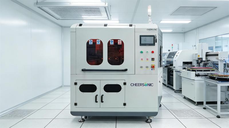
Cheersonic is the leading developer and manufacturer of ultrasonic coating systems for applying precise, thin film coatings to protect, strengthen or smooth surfaces on parts and components for the microelectronics/electronics, alternative energy, medical and industrial markets, including specialized glass applications in construction and automotive.
Our coating solutions are environmentally-friendly, efficient and highly reliable, and enable dramatic reductions in overspray, savings in raw material, water and energy usage and provide improved process repeatability, transfer efficiency, high uniformity and reduced emissions.
Chinese Website: Cheersonic Provides Professional Coating Solutions
