
Mask Version
Mask Version – Spray Coating Photoresist – Cheersonic
Also known in the industry as photomask, mask, English name MASK or PHOTOMASK), material: quartz glass, metal chrome and photosensitive glue, the product is made of quartz glass as the substrate, on which a layer of metal chrome and photosensitive Glue becomes a kind of photosensitive material. The designed circuit pattern is exposed on the photosensitive glue through electronic laser equipment. The exposed area will be developed, and the circuit pattern will be formed on the metal chrome, which will become a light similar to the exposed negative film. The reticle is then used to project and position the integrated circuit, and the projected circuit is photoetched by the integrated circuit lithography machine. The production and processing steps are: exposure, development, photoresist removal, and finally applied to photoetching.
Structure
Solid structure: Image on a quartz glass sheet of chromium metal film covered with an image of an integrated circuit.
Reticle: When the chrome-coated glass can only partially cover the wafer, it is called a reticle, and the pattern is usually enlarged by 4 times, 5 times or 10 times.
Mask: When the image on the chrome-coated glass covers the entire wafer, it is called a mask.
Photolithography
Photolithography (English: photolithography) is an important step in the semiconductor device manufacturing process. This step uses exposure and development to carve geometric patterns on the photoresist layer, and then transfer the pattern on the photomask to the location through the etching process. on the substrate. The substrate mentioned here not only includes silicon wafers, but also other metal layers and dielectric layers, such as glass and sapphire in SOS.
First, through a metallization process, a metal layer only a few nanometers thick is placed on the silicon substrate. This layer of metal is then covered with a layer of photoresist. This layer of photoresist can be dissolved by a specific solution (developer) after exposure (usually ultraviolet light). The photoresist can be selectively illuminated (exposed) by passing specific light waves through a photomask onto the photoresist. The irradiated areas are then dissolved away using the aforementioned developer, so that the pattern on the photomask appears on the photoresist. Some properties of the remaining part of the photoresist are usually improved by drying measures.
After the above steps are completed, the substrate can be selectively etched or ion implanted, and the undissolved photoresist will protect the substrate from being changed during these processes.
After the etching or ion implantation is completed, the final step of photolithography, that is, the removal of the photoresist, is performed to facilitate other steps in the fabrication of the semiconductor device. Typically, many lithography processes are performed throughout the manufacturing process of a semiconductor device. The process of producing complex integrated circuits may require as many as 50 photolithographic steps, while the number of photolithographic steps required to produce thin films will be less.
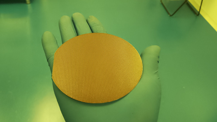
Ultrasonic spraying technology is used for semiconductor photoresist coating. Compared with traditional coating processes such as spin coating and dip coating, it has the advantages of high uniformity, good encapsulation of microstructures, and controllable coating area. In the past 10 years, it has been fully demonstrated that the 3D microstructure surface photoresist coating using ultrasonic spraying technology, the prepared photoresist coating is significantly higher than the traditional spin coating in terms of microstructure wrapping and uniformity Craft.
The ultrasonic spraying system can precisely control the flow rate, coating speed and deposition volume. Low-speed spray shaping defines atomized spray as a precise and controllable pattern to avoid excessive spray when producing a very thin and uniform layer. The ultrasonic spray system can control the thickness from sub-micron to more than 100 microns, and can coat any shape or size.
