
Manufacturing and Coating Process of Sensor Electrode
In the production process of various electronic devices (such as sensors, flexible circuits, etc.), substrate preparation, electrode fabrication, and coating process are the core links that lay the foundation for device performance, stability, and service life. The three need to be closely connected and strictly controlled to ensure that the final product meets the usage requirements.
Substrate preparation
As the basic load-bearing structure of the device, the substrate not only needs to provide stable support for subsequent electrodes and functional layers, but also needs to adapt to the physical and chemical environment during the processing. Its performance directly affects the overall reliability of the device.
1. Common substrate characteristics
PET (Polyethylene terephthalate): As the mainstream choice for flexible substrates, it has excellent mechanical toughness, can withstand a certain degree of bending and folding, and is lightweight and resistant to corrosion from most conventional chemical reagents; At the same time, it has good dimensional stability and is not easily deformed in medium and low temperature processing environments, making it suitable for use in flexible electronics, portable devices, and other scenarios.
PVC (polyvinyl chloride): With outstanding cost economy and low processing difficulty, it can be quickly made into substrates of different shapes through cutting, stamping, and other methods; However, its high temperature resistance is weak, and its long-term use temperature needs to be controlled below 60 ℃. Its insulation performance is slightly inferior to PET, making it more suitable for cost sensitive and mild environment non high precision devices.
Ceramic substrate: It has extremely high insulation strength and thermal conductivity, can withstand high temperatures (usually above 500 ℃) and drastic temperature changes, and has excellent surface flatness; However, the material is brittle and heavy, mainly used for high-power devices and precision electronic components in high-temperature working environments, such as industrial detection sensors, power modules, etc.
2. Core requirements for substrate
Insulation: The volume resistivity of the substrate should not be less than 10 Ω· cm to avoid signal interference or functional failure between electrodes due to leakage, especially in high-precision detection devices where insufficient insulation can directly affect data accuracy.
Surface smoothness: The surface roughness (Ra) should be controlled within 0.5 μ m. If there are protrusions, depressions, or scratches, it will cause uneven coating thickness, conductive layer fracture, and even electrode short circuit in the subsequent coating; Some high-precision scenes require polishing treatment to further improve surface smoothness.
Processing tolerance: It should be able to withstand the mechanical pressure (usually 0.1-0.5 MPa) during subsequent printing, the high temperature of baking and curing (100-150 ℃), and the chemical infiltration of coating materials without cracking, deformation, dissolution, or material aging.
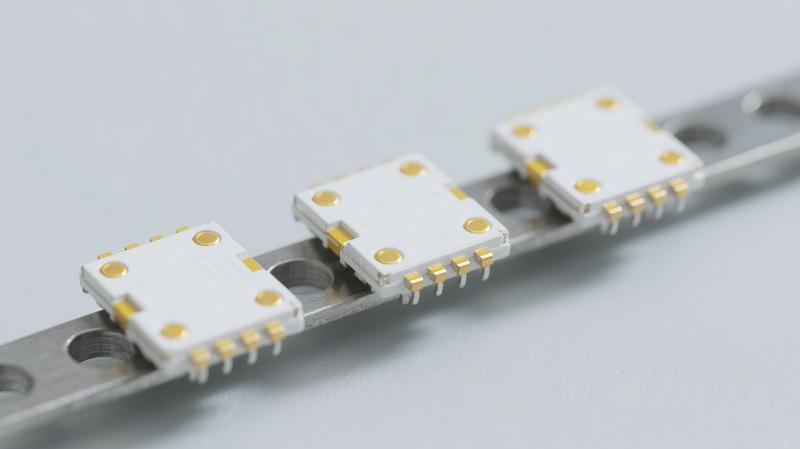
Electrode fabrication
The electrode is the core functional layer of the device for achieving electrical signal transmission, energy conversion, or signal detection. It is necessary to select suitable conductive materials according to the device application to ensure conductivity, stability, and compatibility with the substrate/functional layer.
Selection and Application of Conductive Materials
1. Carbon ink
- Core application: As the preferred material for working electrodes and counter electrodes, it is suitable for most conventional electronic devices and sensors.
- Advantages: Stable conductivity (usually with a volume resistivity of 10 ⁻² -10 ⁻Ω· cm), low cost, strong chemical inertness, and resistance to reactions with subsequent functional layers (such as sensitive films and electrolytes); The particle size (usually 50-200nm) and dispersibility of carbon particles in ink can be controlled, and different coating processes can be adapted by adjusting the formula to form a uniform conductive layer.
- Applicable scenarios: environmental detection sensors, signal transmission electrodes for flexible circuits, low-cost electronic tags, etc.
2. Silver/AgCl ink
- Core application: Specially used as a reference electrode material, it is a key component of potential detection devices such as pH sensors and ion sensors.
- Advantage features: It has strong potential stability and can provide a constant reference potential at room temperature and pressure (approximately 0.222V vs standard hydrogen electrode under standard conditions). It can accurately calibrate the potential signal of the working electrode and reduce detection errors; The molar ratio of silver to silver chloride in the ink material should be strictly controlled at around 1:1, and a binder should be added to enhance the adhesion with the substrate and avoid detachment during use.
- Caution: Store in a dry and dark environment to prevent oxidation of silver components or moisture absorption failure of silver chloride, which may affect potential stability.
3. Gold/Platinum Ink
- Core application: Used in special scenarios with high requirements for sensitivity and biocompatibility, as a working electrode or counter electrode.
- Advantages and characteristics: Excellent conductivity (the volume resistivity of gold is about 2.4 × 10 ⁻⁸Ω· cm, and platinum is about 10.6 × 10 ⁻⁸Ω· cm), which can reduce electrode impedance, improve signal response speed and detection sensitivity; At the same time, it has excellent biocompatibility and will not cause immune reactions or toxicity when in contact with biological tissues or body fluids. It also has strong corrosion resistance and can be used for long-term immersion in electrolytes or biological samples.
- Applicable scenarios: Core electrodes for biosensors (such as blood glucose detection, cell potential monitoring devices) and high-precision electrochemical analysis instruments.
Coating process
The coating process is a key step in accurately transforming conductive materials into electrode structures, which requires the rational selection of coating methods, control of curing conditions, and multi-layer stacking sequence to ensure the conductivity, structural integrity, and interlayer insulation of the electrodes.
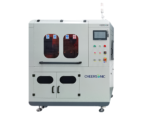
1. Ultrasonic coating process
- Working principle: Using ultrasonic vibration (usually 20-100kHz) to atomize conductive ink into micrometer sized droplets, and then precisely spraying the atomized ink onto the surface of the substrate through high-pressure airflow to form a uniform wet film; Compared to traditional scraper coating and screen printing, ultrasonic coating can achieve finer thickness control (wet film thickness can be controlled between 5-50 μ m), and has a high ink utilization rate (over 90%), making it less prone to defects such as bubbles and pinholes.
- Key parameters: The ultrasonic power and jet pressure need to be adjusted according to the ink viscosity (usually controlled between 10-100cP). When the viscosity is high, the ultrasonic power needs to be increased to ensure atomization effect; The coating speed should match the substrate transport speed (usually 0.5-2m/min) to avoid coating overlap or gaps and ensure the accuracy of the electrode pattern.
2. Baking and curing
- Purpose: To evaporate the solvent in the conductive ink through high-temperature heating, while promoting the tight bonding of conductive particles (such as carbon and silver), forming a stable solid conductive layer, and improving conductivity and adhesion.
- Process parameters: The curing temperature should be strictly controlled at 100-150 ℃. If the temperature is too low, it will cause solvent residue, increase the resistivity of the conductive layer, and decrease the adhesion; If the temperature is too high, it may cause deformation of the substrate (such as PET substrate softening when it exceeds 150 ℃) or oxidation of conductive materials (such as silver ink easily generating silver oxide at high temperatures, reducing conductivity). The curing time is usually 30-60 minutes, which needs to be adjusted according to the coating thickness. For thick films, the time needs to be extended to ensure sufficient solvent evaporation.
- Auxiliary measures: Some ink materials sensitive to oxidation (such as platinum ink) need to be cured in an inert gas (such as nitrogen, argon) atmosphere to prevent metal particles from oxidizing; After curing, it is necessary to cool to room temperature before proceeding with subsequent operations to avoid coating cracking caused by thermal stress.
3. Multi layer process
- Stacking order: It is necessary to follow the principle of “function priority, precise positioning”. Usually, the working electrode (core reaction area, which needs to accurately correspond to the detection or signal acquisition area of the device) is coated first, and after it solidifies, the reference electrode is coated (close to the working electrode, shorten the potential detection path, and reduce signal loss), and finally the counter electrode is coated (forming a current circuit, maintaining a certain distance from the working electrode to avoid short circuits).
- Insulation layer treatment: If the device has multiple sets of electrodes or needs to be isolated from the external environment, an insulation layer (commonly used materials include epoxy resin, polyimide, etc.) should be coated after the electrode layer is cured; The insulation layer needs to cover the non electrode area, only exposing the working end face of the electrode. After coating, it needs to be cured again at 80-120 ℃ to ensure insulation performance and adhesion.
- Interlayer control: During the multi-layer coating process, it is necessary to ensure the alignment accuracy of each layer (with a deviation of less than 10 μ m), which can be achieved through substrate positioning marks or visual alignment systems; After the adjacent layers are cured, surface cleaning is required to remove residual impurities and prevent poor interlayer bonding or short circuits.

About Cheersonic
Cheersonic is the leading developer and manufacturer of ultrasonic coating systems for applying precise, thin film coatings to protect, strengthen or smooth surfaces on parts and components for the microelectronics/electronics, alternative energy, medical and industrial markets, including specialized glass applications in construction and automotive.
Our coating solutions are environmentally-friendly, efficient and highly reliable, and enable dramatic reductions in overspray, savings in raw material, water and energy usage and provide improved process repeatability, transfer efficiency, high uniformity and reduced emissions.
Chinese Website: Cheersonic Provides Professional Coating Solutions
