
Lithography Process Summary
Lithography Process Summary – Lithography Coating System – Cheersonic
1. Optical lithography is a patterning process, which uses ultraviolet light to transfer the pattern designed on the lithography or scaled lithography to the photoresist temporarily coated on the surface of the product.
2. Positive photoresist will become soluble after UV light; negative photoresist will become insoluble due to polymer crosslinking. Positive photoresists are more commonly used because of their higher resolution.
3. The photolithography dumpling is composed of polymerization, sensitizer, solvent and additives.
4. The basic optical lithography process flow is: epi cleaning, pre-baking and HMOS primer coating, photoresist spin coating, soft baking, alignment and exposure, post-exposure baking, removal of optical edge beads, Development, Baking and Pattern Inspection,
5. Wafer cleaning can reduce contamination and improve photoresist adhesion to the
6. Pre-baking can remove the moisture on the wafer surface, and the HMDS primer layer can help the photoresist adhere to the surface of the wafer.
7. Convective constant temperature test box, infrared oven, microwave oven and heating plate can be used for baking process. Heated plates are most commonly used in advanced semiconductor factories.
8. Spin coating is the most commonly used photoresist coating process. Photoresist thickness and uniformity and spin rate, spin rate increase.
9. The photoresist thickness and uniformity are related to the spin rate, the way the spin rate increases, the photoresist temperature, the wafer stability, the air flow rate and the gas temperature.
10. Baking will remove most of the solvent in the lithography dumpling and make it solid.
11. Overbaking in the soft baking process will cause photolithography to polymerize and affect exposure sensitivity.
12. Insufficient bake in soft bake process can cause blurred images due to excess solvent and photoresist peeling during etching or ion implantation process.
13. Connected exposure machines, proximity exposure machines, projection exposure machines and steppers are used for the alignment of exposure systems. Steppers have the highest resolution and are therefore most commonly used in advanced semiconductor processes.
14. Since the photoresist molecules are moved by heat, the post-exposure bake can alleviate the standing wave effect.
15. The developing process will dissolve the exposed positive photoresist during the developing process. The development process is very temperature sensitive. 16. The hard bake will drive the residual solvent from the photoresist, improving the resistance to clouding and ion implantation, as well as the adhesion of the photoresist. Underbaking can cause photoresist loss during the etch process; overbaking can cause light to flow and affect resolution.
17. Baking, coating and developing processes are usually carried out together with the wafer track system, which is integrated with the stepper. The wavelength commonly used in IC manufacturing is ArF 193nm.
19. Combining immersion lithography and double-sided or multi-sided patterned drum technology to apply optical lithography development to the 22nm technology node, and can scale to the 16nm node or smaller. While optical lithography has its limits, patterning has no limits.
20. ELV, EBDW lithography and NIL technology are candidates for next-generation lithography.
21. EUV lithography technology can replace optical lithography technology in the future related patterning process, most likely first for the contact layer patterning of 22nm NAND memory.
Cheersonic’s ultrasonic spraying technology is used for semiconductor photoresist coating. Compared with traditional coating processes such as spin coating and dip coating, it has the advantages of high uniformity, good encapsulation of microstructures, and controllable coating area. In the past 10 years, it has been fully demonstrated that the 3D microstructure surface photoresist coating using ultrasonic spraying technology, the prepared photoresist coating is significantly higher than the traditional spin coating in terms of microstructure wrapping and uniformity Craft.
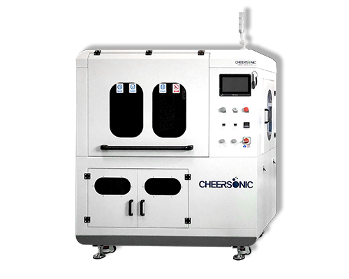
The ultrasonic spraying system can precisely control the flow rate, coating speed and deposition volume. Low-speed spray shaping defines atomized spray as a precise and controllable pattern to avoid excessive spray when producing a very thin and uniform layer. The ultrasonic spray system can control the thickness from sub-micron to more than 100 microns, and can coat any shape or size.
