
Lithography of Chip Manufacturing Technology
Lithography of Chip Manufacturing Technology – Photoresist Coater – Cheersonic
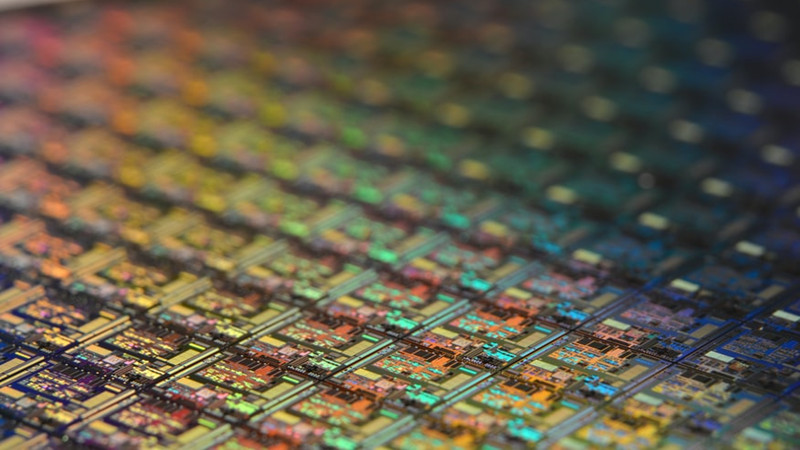
In the manufacturing process of integrated circuits, there is an important link – lithography, it is because of it that we can realize functions on tiny chips.
Photolithography is an important step in the manufacturing process of semiconductor devices. This step uses exposure and development to delineate geometric structures on the photoresist layer, and then transfers the patterns on the photomask to the substrate through an etching process.
The basic principle of lithography is to use the characteristics of photoresist (or photoresist) to form corrosion resistance due to photochemical reaction after being exposed to light, and to carve the pattern on the mask onto the processed surface. The main steps of photolithography semiconductor chip silicon dioxide are: 1. Coating photoresist; 2. Registering the mask and exposing it; 3. Dissolving the unphotosensitive photoresist layer with developer; 4. Using The etching solution dissolves the silicon dioxide layer without photoresist protection; 5. Removes the photoresist layer that has been exposed to light.
etching
Etching is a process in semiconductor device fabrication that utilizes chemical means to selectively remove specific portions of a deposited layer. Etching is very important for the electrical properties of the device. If there is a mistake in the etching process, the silicon wafer that is difficult to recover will be scrapped, so strict process control must be carried out. Each layer of a semiconductor device undergoes multiple etching steps.
Ion Implantation
Ion implantation is a technique in which specific ions are accelerated in an electric field and then embedded in another solid material. Ion implantation can cause nuclear transitions, or change the crystal structure of certain solid materials.
photoresist removal
The main function of the photoresist is to protect the portion of the substrate under the photoresist when chemical or mechanical processing processes are performed over the entire area. Therefore, after etching or ion implantation, the photoresist is no longer required as a protective layer, and the photoresist should be completely removed. This step is referred to as removing the glue. Degumming is divided into wet degumming and dry degumming.
In addition to these main processes, some auxiliary processes are often used, such as uniform etching of a large area to reduce the thickness of the substrate, or to remove uneven edges. Generally, in the production of semiconductor chips or other components, a substrate needs to be repeated many times for photolithography.
The ultrasonic coating system can use advanced layering technology to precisely control the flow rate, coating speed and deposition amount. Low-speed spray forming defines an atomizing spray as a precise, controllable pattern, avoiding excessive spraying when producing very thin and uniform layers. It turns out that direct spraying using ultrasonic technology is a reliable and effective way to deposit photoresist on 3D microstructures, thereby reducing equipment failures caused by excessive metal exposure to etchant.
Ultrasonic spray systems have proven to be suitable for a variety of applications that require uniform, repeatable photoresist or polyimide film coatings. Cheersonic’s coating system can control thicknesses from sub-micron to more than 100 microns, and can coat any shape or size. It is a feasible alternative to other coating technologies such as spin coating and traditional spray coating.
Cheersonic’s non-blocking ultrasonic coating technology is known for its ultra-thin micron-layer coatings of functional and protective materials. The ultrasonic vibration of the nozzle effectively dispersed the particles in the suspension and produced a very uniform particle dispersion in the film layer, while the conductive particles did not settle out of the suspension.
