
How Perovskite Cells Work
How Perovskite Cells Work – Uniform Coatings of Perovskite Solar Cell – Cheersonic
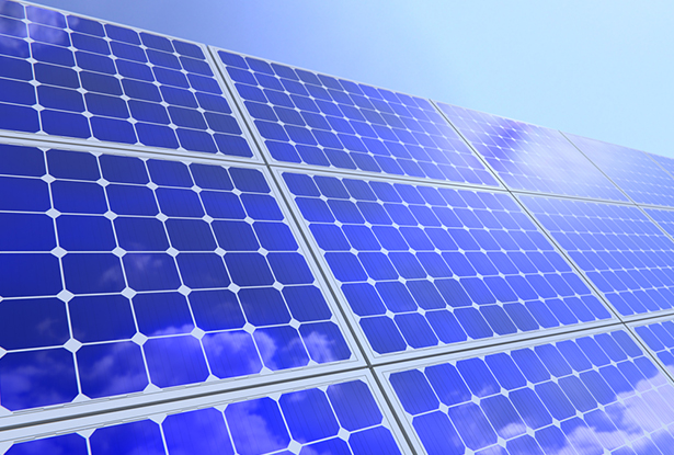
Perovskite cells are the breakthrough representative of the new generation of high-efficiency thin-film solar cells, which have the characteristics of simple preparation process and good defect tolerance. By combining single cells, the spectral response of the cell can be effectively broadened, and the ultimate photoelectric conversion efficiency is higher than that of single-junction cells.
A common perovskite/silicon heterojunction stack cell consists of three parts: a perovskite top cell, an intermediate connection layer (tunnel junction) and a silicon heterojunction bottom cell.
The working principle of each component is as follows:
TCO: transparent conductive film glass, used as the anti-reflection film of the battery to reduce the reflection loss of light and improve the conversion efficiency of the battery.
Electron transport layer: plays the role of transporting electrons and blocking holes.
Perovskite absorption layer: The effective optical absorption layer of the perovskite top cell mainly absorbs light in the short-wavelength range (300-800Nm).
Hole transport layer: blocks electrons and enhances hole transport.
Intermediate connection layer (tunnel junction): Both perovskite cells and silicon heterojunction cells have a P-N structure, and direct series contact interfaces will form a reverse-biased PN junction, resulting in voltages that cancel each other out and make them non-conductive. The tunnel junction is also a P-N structure, which can generate tunnel current and connect two sub-cells.
Heterojunction: P-type semiconductor and N-type semiconductor are fabricated on the same silicon substrate, and the space charge region (PN junction) formed at the interface has unidirectional conductivity.
Silicon-based heterojunction: There are both crystalline and amorphous silicon in the silicon heterojunction cell with an intrinsic amorphous layer. Amorphous silicon can better achieve passivation effect, improve open circuit voltage and conversion efficiency.
Silicon heterojunction bottom cell: crystalline silicon (c-Si) is used as the optical absorption layer of the bottom cell to absorb light in the long-wavelength range (800-1200Nm).
Ultrasonic spray technology has been proven successful for depositing thin film solar cell coatings of anti-reflection layers, TCO coatings, Buffer layer coatings, PEDOT, and active layers in thin film and perovskite solar cell manufacturing. Our coating solutions are environmentally-friendly, efficient and highly reliable, and enable dramatic reductions in overspray, savings in raw material, water and energy usage and provide improved process repeatability, transfer efficiency, high uniformity and reduced emissions.
Chinese Website: Cheersonic Provides Professional Coating Solutions
