Difficulties of Photosensitive Polyimide
The production of PSPI photoresist is in the middle of the industrial chain structure. It is an ideal insulating material in the field of electronics and microelectronics. It is one of the most important electronic chemical materials in the fields of optoelectronics and microelectronics such as display panels, LED packaging, semiconductors, etc. It is widely used as interlayer insulation, surface passivation, stress buffering, and radiation shielding.
1. Difficulties in the basic performance of materials
PI materials generally need to be fully cured under high temperature conditions above 350 degrees, but in the actual wafer application process, as the chip area increases and the wafer thickness decreases, the demand for low curing temperature is strong. How to obtain PSPI materials that can be cured below 250 degrees and still have good performance is extremely difficult.
2. Difficulties in the engineering application of materials
PSPI is both a photolithography process material and a chip packaging structure material. After the process is completed, it is finally retained in the wind device. To ensure its stability on mobile phone chips and car chips for decades, stringent requirements are placed on the reliability, purity, and various aspects of the material.
3. Testing cycle barriers for material applications
PSPI, as a direct material for front-end IC, back-end advanced packaging, MEMS and organic light-emitting diode (OLED) display, will be permanently retained inside the chip and device, resulting in a relatively long product verification cycle, ranging from 6 months to 2-3 years. At the same time, it is also necessary to pass multiple reliability tests. The long test cycle means that it takes a long time for suppliers to enter the downstream customer supply chain system, which has established a certain first-mover moat for the first-entering companies.
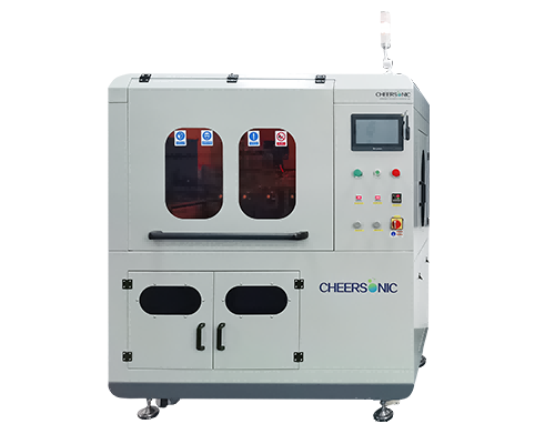
Ultrasonic spraying systems have been proven to be used in various applications that require uniform and repeatable photoresist or polyimide film coatings. The thickness control range is from submicron to more than 100 microns, and any shape or size can be coated.
Ultrasonic spraying technology is used for semiconductor photoresist coating. Compared with traditional coating processes such as spin coating and dip coating, it has the advantages of high uniformity, good encapsulation of microstructures, and controllable coating area. In the past 10 years, it has been fully demonstrated that the 3D microstructure surface photoresist coating using ultrasonic spraying technology, the prepared photoresist coating is significantly higher than the traditional spin coating in terms of microstructure wrapping and uniformity Craft.
The ultrasonic spraying system can precisely control the flow rate, coating speed and deposition volume. Low-speed spray shaping defines atomized spray as a precise and controllable pattern to avoid excessive spray when producing a very thin and uniform layer. The ultrasonic spray system can control the thickness from sub-micron to more than 100 microns, and can coat any shape or size.
About Cheersonic
Cheersonic is the leading developer and manufacturer of ultrasonic coating systems for applying precise, thin film coatings to protect, strengthen or smooth surfaces on parts and components for the microelectronics/electronics, alternative energy, medical and industrial markets, including specialized glass applications in construction and automotive.
Our coating solutions are environmentally-friendly, efficient and highly reliable, and enable dramatic reductions in overspray, savings in raw material, water and energy usage and provide improved process repeatability, transfer efficiency, high uniformity and reduced emissions.
Chinese Website: Cheersonic Provides Professional Coating Solutions


