Applications of Photosensitive Polyimide
Photosensitive polyimide (PSPI) is a type of polymer material that has both heat resistance and photosensitive properties. It is a very important semiconductor material and a very stuck material. Due to its electrical insulating properties, it protects semiconductor circuits from physical and chemical conditions.
Photosensitive polyimide mainly plays two major roles in the electronic field: photoresist and electronic packaging.
1. As photoresist
As a photoresist, “polyimide photoresist” can be obtained by adding sensitizers, stabilizers, etc. to photosensitive polyimide. Under the radiation of ultraviolet light, alpha rays, X-rays, etc., the structure of the irradiated part will change, and it can be dissolved in the corresponding solvent and can be used to make precise patterns.
Compared with traditional photoresists, the most significant difference is that after the photolithography is patterned, the photosensitive polyimide photoresist remains in a specific area to form the dielectric insulation layer required for the device, while ordinary photoresist will Its pattern will be removed after it is transferred to the underlying material.
At the same time, because polyimide itself has good dielectric properties, it does not need to be coated with a photoblocker that only functions as a working medium when used, which can greatly shorten the process and improve production efficiency. While saving material costs, it also significantly shortens the integrated circuit manufacturing process and improves photolithography pattern accuracy and yield.
2. As electronic packaging material
In the direction of electronic packaging, for advanced packaging of semiconductors, it can be used for stress buffer layers, insulating layers and interlayer insulating materials. Wafer packaging (WLCSP), fan-out wafer packaging (F0-WLP), flip chip (FC BGA), 2.5D packaging, 3D packaging, etc.
In display devices (such as AMOLED displays), as array BOM materials, it is widely used in planarization layer (PLN), pixel definition layer (PDL), and support layer (PS) insulation films to improve interlayer insulation and reduce display chromatic aberration. .
In microelectromechanical systems (MEMS) systems, PSPI has become an ideal dielectric insulation material between layers and metal lines in MEMS manufacturing, as well as a structural material for the construction of MEMS system components. The dielectric insulating layers of traditional MEMS, such as silicon oxide and silicon nitride, require special deposition processes and patterning steps. Using PSPI as the insulating layer not only simplifies the manufacturing process, but also has excellent properties, such as thermal stability, chemical resistance, low dielectric constant and low residual stress.
With the miniaturization, thin film, high performance, multi-function, high reliability and low cost of electronic products, market demand has increased the density of integrated circuit packaging, and the requirements for IC packaging materials are also increasing. With the arrival of the era of large chips, the original metal and ceramic material packaging technology has been greatly impacted. Electronic packaging materials represented by epoxy resin, polyimide resin, etc. are gradually emerging as important IC packaging materials.
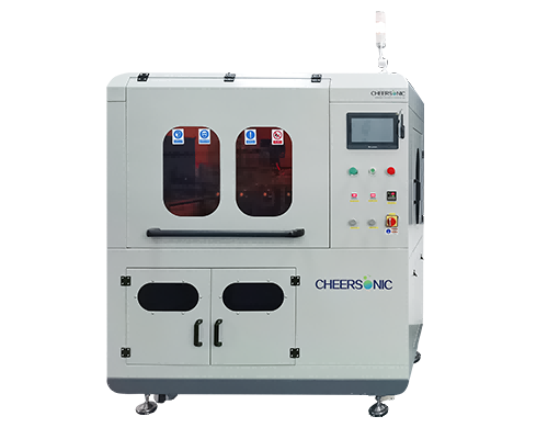
Ultrasonic spraying systems have been proven to be used in various applications that require uniform and repeatable photoresist or polyimide film coatings. The thickness control range is from submicron to more than 100 microns, and any shape or size can be coated.
Ultrasonic spraying technology is used for semiconductor photoresist coating. Compared with traditional coating processes such as spin coating and dip coating, it has the advantages of high uniformity, good encapsulation of microstructures, and controllable coating area. In the past 10 years, it has been fully demonstrated that the 3D microstructure surface photoresist coating using ultrasonic spraying technology, the prepared photoresist coating is significantly higher than the traditional spin coating in terms of microstructure wrapping and uniformity Craft.
The ultrasonic spraying system can precisely control the flow rate, coating speed and deposition volume. Low-speed spray shaping defines atomized spray as a precise and controllable pattern to avoid excessive spray when producing a very thin and uniform layer. The ultrasonic spray system can control the thickness from sub-micron to more than 100 microns, and can coat any shape or size.
About Cheersonic
Cheersonic is the leading developer and manufacturer of ultrasonic coating systems for applying precise, thin film coatings to protect, strengthen or smooth surfaces on parts and components for the microelectronics/electronics, alternative energy, medical and industrial markets, including specialized glass applications in construction and automotive.
Our coating solutions are environmentally-friendly, efficient and highly reliable, and enable dramatic reductions in overspray, savings in raw material, water and energy usage and provide improved process repeatability, transfer efficiency, high uniformity and reduced emissions.
Chinese Website: Cheersonic Provides Professional Coating Solutions


