
Advanced Packaging Photoresist Coatings
Panel-Level Packaging: Advanced Photoresist Coating Technology Empowering Semiconductor Advanced Processes
With the rapid iteration of AI computing power and the continuous upgrading of semiconductor chip performance, advanced packaging has become a core track to break through the bottlenecks of chip manufacturing processes and improve device integration. As a disruptive packaging technology, Panel-Level Packaging (PLP) is gradually replacing traditional wafer packaging due to its high efficiency and low-cost advantages. Meanwhile, advanced packaging photoresist coating technology serves as a crucial core material that supports the implementation of PLP processes and enables precision wiring.
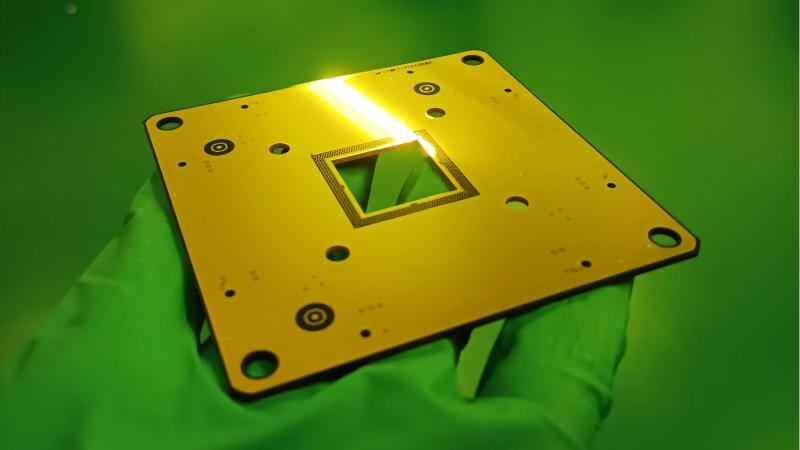
Different from traditional circular wafer packaging, PLP adopts large-size rectangular panel substrates, which completely breaks the limitation of wafer dimensions, greatly improves the utilization rate of chip layout, and significantly increases the number of chips processed in a single batch. It effectively reduces mass production costs and meets the large-scale production demands of high-end chips, automotive electronics, and smart terminals. However, large-size panels also bring process challenges including substrate warpage, uneven temperature difference, and difficult pattern precision control, placing higher requirements on the stability and adaptability of supporting photoresist coatings.
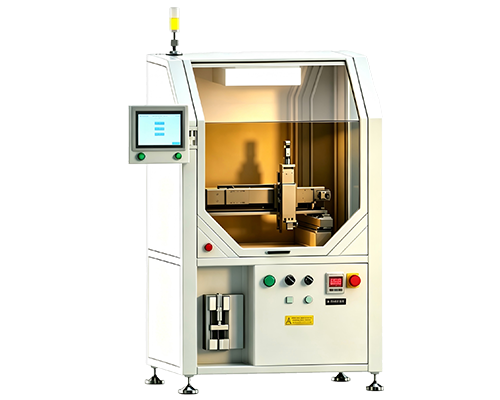
Special photoresist coatings for advanced packaging act as the core support for PLP processes, mainly applied in the fabrication of Redistribution Layers (RDL) to accurately transfer circuit patterns and realize precise inter-chip interconnection. The new-type photoresist adapted for PLP overcomes the shortcomings of traditional materials. It is compatible with multiple coating processes such as slot-die coating and spin coating, features a wide film thickness adaptation range, and can stably achieve micron-level fine pattern resolution. In addition, the novel fluorine-free and Post-Exposure Bake (PEB)-free photoresist effectively solves the problem of pattern deformation caused by uneven temperature differences on large panels, while possessing excellent copper plating stability and eco-friendly properties.
Furthermore, this special photoresist delivers outstanding exposure delay stability and can form vertically regular pattern contours, ensuring the reliability of subsequent metallization and packaging molding processes. It is perfectly applicable to 2.5D and 3D advanced integrated packaging scenarios. As a core supporting material for PLP technology, advanced photoresist coatings are continuously upgraded and iterated to steadily overcome the precision and stability challenges of large-size packaging.
In the future, as semiconductor packaging evolves toward higher integration, higher precision and lower cost, PLP technology will achieve comprehensive popularization. The continuous innovation of advanced packaging photoresist coating materials will become a core driving force for upgrading the semiconductor advanced packaging industry and empowering the development of high-end electronic industries.
About Cheersonic
Cheersonic is the leading developer and manufacturer of ultrasonic coating systems for applying precise, thin film coatings to protect, strengthen or smooth surfaces on parts and components for the microelectronics/electronics, alternative energy, medical and industrial markets, including specialized glass applications in construction and automotive.
Our coating solutions are environmentally-friendly, efficient and highly reliable, and enable dramatic reductions in overspray, savings in raw material, water and energy usage and provide improved process repeatability, transfer efficiency, high uniformity and reduced emissions.
Chinese Website: Cheersonic Provides Professional Coating Solutions
