
Introduction to ITO Conductive Glass
Basic definition and core characteristics of ITO conductive glass
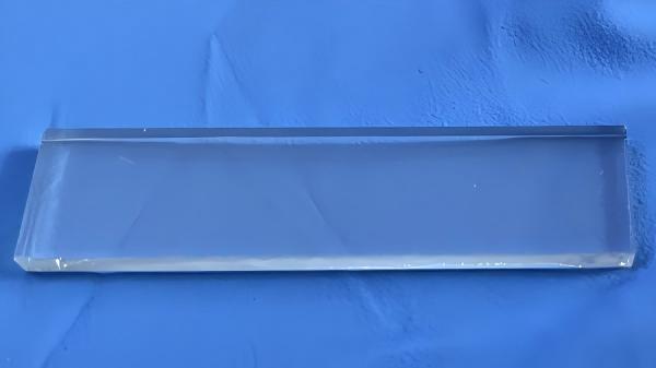
ITO conductive glass is a transparent conductive material made by sequentially depositing a silicon dioxide (SiO ₂) barrier layer and an indium tin oxide (ITO) thin film on a sodium calcium based or silicon boron based substrate glass through processes such as magnetron sputtering and ultrasonic spraying. Among them, ITO has the characteristics of forbidden bandwidth, high visible spectral transmittance, and low resistivity, and is widely used in flat panel display devices (LCD, PDP, OLED, touch screen), solar cells, special function window coatings, and optoelectronic devices. It is a key transparent conductive electrode material for optoelectronic devices.
Its core features are as follows:
Transparency: High transmittance in the visible light range, it does not affect the optical performance of the device when used as a transparent conductive layer;
Conductivity: With low resistance, it can stably conduct current and meet the conductivity requirements of electronic devices;
Corrosion resistance: able to resist the erosion of most chemical substances, extending the service life and stability of materials;
Mechanical strength: Although slightly more brittle than conventional glass, its fragility can be reduced through process optimization;
Thermal stability: It maintains stable conductivity even in high temperature environments and is suitable for various processing scenarios.
Classification of ITO conductive glass
According to application requirements, ITO conductive glass can be classified into multiple dimensions:
Classified by resistance value
High resistance glass (150-500 ohms): used for electrostatic protection and touch screen production;
Ordinary glass (60~150 ohms): suitable for TN LCD displays and electronic anti-interference scenarios;
Low resistance glass (<60 ohms): used in STN LCD displays and transparent circuit boards.
Classified by size and thickness
Size specifications: Common sizes include 14 “× 14”, 14 “× 16”, 20 “× 24”, etc;
Thickness specifications: 2.0mm, 1.1mm, 0.7mm, 0.55mm, 0.4mm, 0.3mm, etc. Among them, thicknesses below 0.5mm are mainly used for STN LCD displays.
Classified by structure and performance
Single sided conductive glass: ITO film only covers one side of the glass, used for smartphones, tablets, touch screens, and LCD displays;
Double sided conductive glass: ITO film covers both sides of the glass, suitable for flat panel displays and solar cells;
Flexible conductive glass: using a special substrate that can bend and maintain conductivity, used for flexible displays and wearable devices;
Customized conductive glass: Adjust the film thickness and resistivity according to the scene (such as high transmittance required for solar cells).
Classified by flatness
It is divided into polished glass (specialized for high-end LCD displays, requiring polishing treatment before sputtering to improve display uniformity) and ordinary glass.
Preparation process of ITO conductive glass
1. Core coating process
Magnetron sputtering process: The mainstream coating method adjusts the distance, temperature, and motion of the target material and glass to control the characteristics of the ITO layer (such as surface smoothness and resistance stability). Please note that some processes can easily cause issues such as “pitting”, high etching spacing (resulting in straight lines or high resistance bands during etching), and microcrystal grooves in the ITO layer.
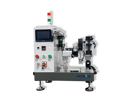
Ultrasonic spraying process: Auxiliary coating technology, which atomizes the coating material into small particles through high-pressure airflow and evenly sprays them on the surface of the substrate. Its advantage lies in the precise and controllable thickness of the film layer, high coating uniformity, which can be used for the fine preparation of SiO ₂ barrier layers or ITO films, especially suitable for high-end LCD displays with high requirements for film flatness.
2. Preparation process of special functional thin films
Electrochemical diffusion process: Glass is placed in an electrochemical treatment device and comes into contact with molten metal/compounds. Under the action of an electric field, molten ions diffuse to the surface of the glass, replacing monovalent alkali metal ions in the glass and changing the chemical composition and properties of the glass surface. Doping superconducting thin films can be prepared.
High temperature ultrasonic spraying and plasma spraying processes: Metal/non-metal and inorganic powders are heated to a molten/semi molten state, atomized and sprayed at high speed onto a glass substrate. Coatings such as YBaCuOx are first prepared, and then superconducting materials are obtained through heat treatment.
Plasma chemical vapor deposition technology: In a vacuum environment, low-pressure gas discharge plasma is used to activate deposited atoms, and through physical or chemical vapor deposition, nano to micron level functional layers are formed on the substrate to enhance the material’s optical and electrical properties.
Electron beam evaporation technology: In a vacuum environment, 5-10kV electron beams bombard the material to be evaporated, causing it to melt and evaporate, and then condense into a film on the substrate. Advantages include: high purity of the film layer, good density, and strong adhesion to the substrate; Wide material selectivity and easy thickness control; Environmentally friendly waste water without exhaust gas; Can be deposited at low temperatures, suitable for organic materials such as PET, PMMA, PC, etc.
Planar magnetron sputtering technology: In a vacuum environment, low-pressure gas discharge plasma accelerates ion bombardment of the target material, causing atomic sputtering and deposition on the substrate, changing the surface function of the material.
ITO conductive film glass production process
Taking ITO conductive film glass for LCD as an example, the core process is as follows (the process for touch screens is slightly different, LCD requires additional multi-level coating such as TiO ₂, Nb ₂ O ₅, and adjusting process parameters):
Cutting and edging: Cut ultra-thin glass below 1.1mm into specified sizes as required, grind edges and chamfers to ensure safety and positioning accuracy in subsequent operations;
Original glass inspection: Check the apparent quality of cut glass (scratches, point defects, edge quality, geometric dimensions), and remove non-conforming products;
Cleaning: Perform multi-step cleaning in the purified environment: cleaning solution roller brush → cleaning solution disc brush → purified water roller brush → purified water disc brush → purified water spray → hot air drying. After passing the inspection, send it to the ultra clean room for coating;
Vacuum coating: glass mounting → adjusting equipment parameters (target voltage, current, temperature, working cycle) → coating SiO ₂ film (blocking sodium ion diffusion) → coating ITO film → unloading;
Finished product inspection: Inspect the apparent quality and electrical performance of each piece, sample and verify key indicators, package and label information according to customer requirements for quality tracking.
About Cheersonic
Cheersonic is the leading developer and manufacturer of ultrasonic coating systems for applying precise, thin film coatings to protect, strengthen or smooth surfaces on parts and components for the microelectronics/electronics, alternative energy, medical and industrial markets, including specialized glass applications in construction and automotive.
Our coating solutions are environmentally-friendly, efficient and highly reliable, and enable dramatic reductions in overspray, savings in raw material, water and energy usage and provide improved process repeatability, transfer efficiency, high uniformity and reduced emissions.
Chinese Website: Cheersonic Provides Professional Coating Solutions
