
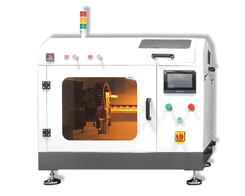
Process of Spraying Photoresist onto a Silicon Wafer
Ultrasonic spraying offers significant advantages in silicon wafer processing. Using high-frequency vibrations, it atomizes the coating into uniform, tiny droplets of 5-30 microns. This creates a uniform coating on the wafer surface with precisely controllable thickness (0.1-5 microns), free of pinholes and buildup, avoiding the uneven thickness and particle agglomeration associated with traditional spraying. Ultrasonic spraying boasts a material utilization rate exceeding 90%, significantly reducing waste of expensive materials such as photoresist and passivation layers. Spraying is free of high-speed airflow impact, preventing damage to the wafer surface or particulate contamination. It is suitable for wafer sizes ranging from 6-12 inches and accommodates a variety of functional coating requirements. Its robust process improves wafer processing yield and is widely used in critical coating processes in semiconductor manufacturing.
The process of spraying photoresist onto a silicon wafer typically uses a spin coating method. The specific steps are as follows:
1. Wafer cleaning: The silicon wafer is cleaned with a chemical solvent and deionized water to remove surface impurities and contaminants.
2. Photoresist preparation: The appropriate photoresist is selected and heated to an appropriate temperature to reduce its viscosity and improve its fluidity.
3. Dispensing: The photoresist is dropped onto the center of the silicon wafer.
4. Spin coating: The wafer is rotated at high speed, allowing the centrifugal force to evenly distribute the photoresist across the wafer surface, forming a uniform film.
5. Soft baking: The photoresist-coated wafer is soft-baked to remove the solvent from the photoresist and improve its adhesion and stability.
6. Cooling: The wafer is cooled to room temperature to solidify the photoresist on the surface.
In addition, in practical applications, to ensure the quality and performance of photoresist, the following points should be noted:
- Selecting the appropriate photoresist: Choose the appropriate photoresist type and brand based on the wafer material, size, and process requirements.
- Controlling coating parameters: This includes rotation speed, acceleration, coating time, etc., to ensure that the photoresist thickness and uniformity meet the requirements.
- Maintaining a clean environment: During the coating process, the environment must be kept clean and dry to avoid contamination from dust and impurities.
- Conducting quality inspections: After coating, the photoresist must be inspected for thickness, uniformity, adhesion, and other factors to ensure it meets the requirements.
About Cheersonic
Cheersonic is the leading developer and manufacturer of ultrasonic coating systems for applying precise, thin film coatings to protect, strengthen or smooth surfaces on parts and components for the microelectronics/electronics, alternative energy, medical and industrial markets, including specialized glass applications in construction and automotive.
Our coating solutions are environmentally-friendly, efficient and highly reliable, and enable dramatic reductions in overspray, savings in raw material, water and energy usage and provide improved process repeatability, transfer efficiency, high uniformity and reduced emissions.
Chinese Website: Cheersonic Provides Professional Coating Solutions
